96SD2-1G800NN-AP3

Apacer Memory Product Specification
1024MB DDR2 SDRAM SO-DIMM
1024MB DDR2 SDRAM SO-DIMM based on 128Mx8 ,8Banks, 1.8V DDR2 SDRAM with SPD
Features
Description
This module is 128M bit x 64x1Rank Double Data Rate SDRAM high density memory modules based on first
generation of
1024MB DDR2 SDRAM respectively.
It consists of eight CMOS
128M x
8 bit with 8banks Double Data Rate SDRAMs in 60Ball FBGA packages
mounted on a 200pin glass-epoxy substrate.
Two 0.1uF decoupling capacitors are mounted on the
printed circuit
board in parallel for each DDR2 SDRAM.
Synchronous design allows precise cycle control with the use of system clock. Data I/O transactions are possible on
both edges of DQS. Range of operating frequencies, programmable latencies and burst lengths allow the same
device to be useful for a variety of high bandwidth, high performance memory system applications.
Performance range
( Bandwidth: 6.4 GB/sec )
Part Number Max Freq. (Clock) Speed Grade
78.02G86.XX2 400MHz(2.5ns@CL6) 800Mbps
JEDECstandard 1.8V ± 0.1V Power Suppl
y
VDDQ = 1.8V± 0.1V
Internal Bank: 8 Ban
k
Posted CAS
Pro
g
rammable CAS Latenc
y
: 3, 4, 5
Pro
g
rammable Additive Latenc
y
: 0, 1 , 2 , 3 and 4
Write Latenc
y(
WL
)
= Read Latenc
y(
RL
)
-1
Burst Len
g
th: 4 , 8
(
Interleave/nibble sequential
)
Pro
g
rammable Sequential / Interleave Burst Mode
Bi-directional Differential Data-Strobe
(
Sin
g
le-ended data-strobe is an optional feature
)
Off-Chip Driver
OCD
Impedance Ad
ustmen
On Die Termination
Refresh and Self Refresh
Average Refesh Period 7.8us
Serial presence detect with EEPROM
Compliance with RoHS
Compliance with CE
Operatin
g
Temperature Ran
g
:
Commercial 0°C TC 85°C
Industrial -40°C TA 85°C
Refresh: auto-refresh, self-refresh
‧─Avera
g
e refresh period
7.8us at 0°C TC 85°C
3.9us at 85°C TC 95°C
Industrial S
y
stem Level -40°C TA 70°C
Apacer Memory Product Specification
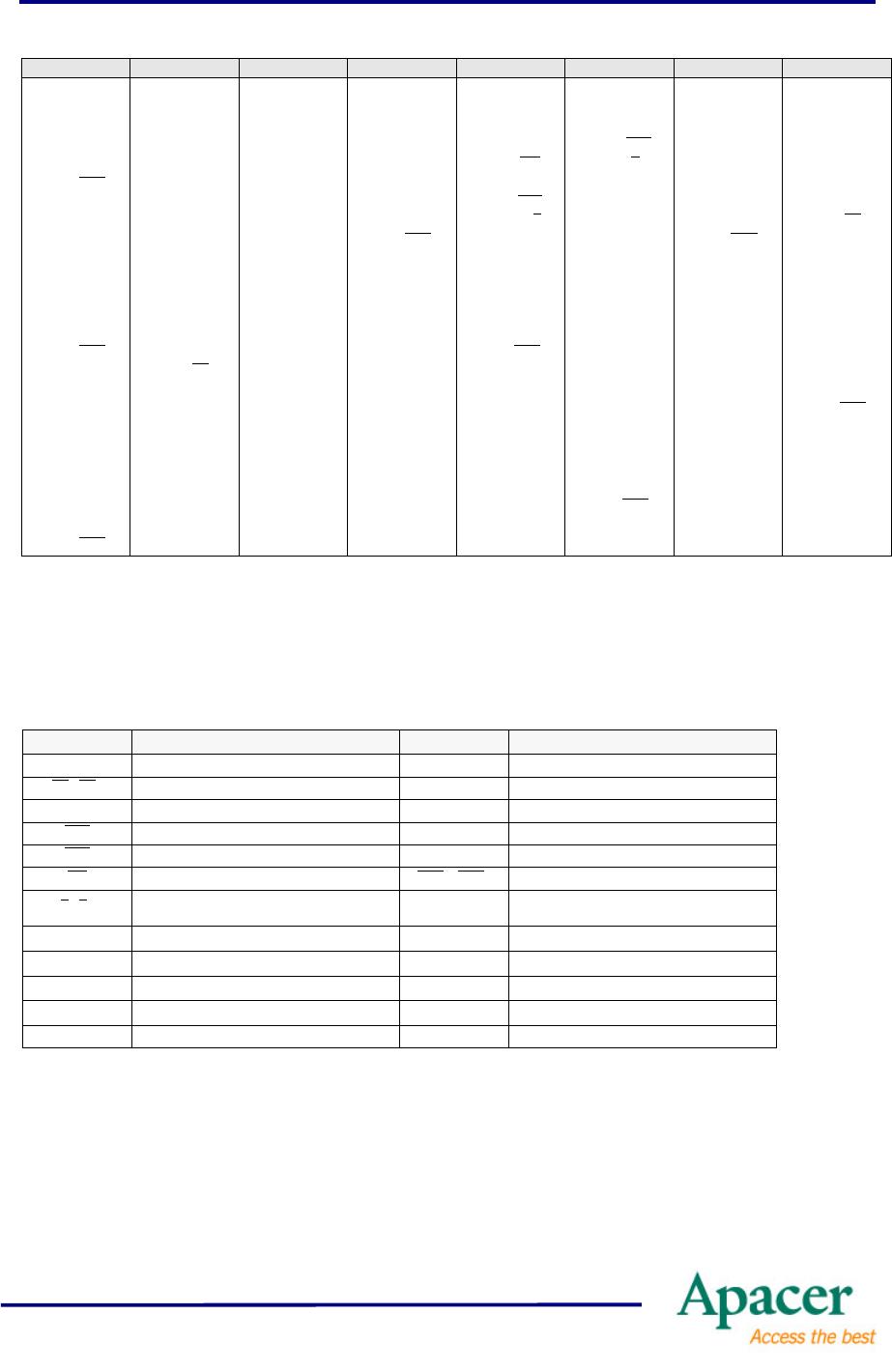
Pin Configurations (Front side/Back side)
Pin Front Pin Back Pin Front Pin Back Pin Front Pin Back Pin Front Pin Back
1
V
REF
2
V
SS
51 DQS2 52 DM2 101 A1 102 A0 151 DQ42 152 DQ46
3
V
SS
4DQ453
V
SS
54
V
SS
103
V
DD
104
V
DD
153 DQ43 154 DQ47
5 DQ0 6 DQ5 55 DQ18 56 DQ22 105 A10/AP 106 BA1 155
V
SS
156
V
SS
7DQ18
V
SS
57 DQ19 58 DQ23 107 BA0 108 RAS 157 DQ48 158 DQ52
9
V
SS
10 DM0 59
V
SS
60
V
SS
109 WE 110 S0 159 DQ49 160 DQ53
11 DQS
012
V
SS
61 DQ24 62 DQ28 111
V
DD
112
V
DD
161
V
SS
162
V
SS
13DQS014 DQ6 63DQ2564DQ29113CAS114 ODT0 163 NC, TEST 164 CK1
15
V
SS
16 DQ7 65
V
SS
66
V
SS
115 NC/S1 116 A13 165
V
SS
166 CK1
17 DQ2 18
V
SS
67 DM3 68 DQS3117
V
DD
118
V
DD
167 DQS6 168
V
SS
19 DQ3 20 DQ12 69 NC 70 DQS3 119 NC/ODT1 120 NC 169 DQS6 170 DM6
21
V
SS
22 DQ13 71
V
SS
72
V
SS
121
V
SS
122
V
SS
171
V
SS
172
V
SS
23 DQ8 24
V
SS
73 DQ26 74 DQ30 123 DQ32 124 DQ36 173 DQ50 174 DQ54
25 DQ9 26 DM1 75 DQ27 76 DQ31 125 DQ33 126 DQ37 175 DQ51 176 DQ55
27
V
SS
28
V
SS
77
V
SS
78
V
SS
127
V
SS
128
V
SS
177
V
SS
178
V
SS
29 DQS1 30 CK0 79 CKE0 80 NC/CKE1 129 DQS4 130 DM4 179 DQ56 180 DQ60
31 DQS1 32 CK
081
V
DD
82
V
DD
131DQS4132
V
SS
181 DQ57 182 DQ61
33
V
SS
34
V
SS
83 NC 84 NC 133
V
SS
134DQ38183
V
SS
184
V
SS
35 DQ10 36 DQ14 85 BA2 86 NC 135 DQ34 136 DQ39 185 DM7 186 DQS7
37 DQ11 38 DQ15 87
V
DD
88
V
DD
137DQ35138
V
SS
187
V
SS
188 DQS7
39
V
SS
40
V
SS
89 A12 90 A11 139
V
SS
140 DQ44 189 DQ58 190
V
SS
41
V
SS
42
V
SS
91 A9 92 A7 141 DQ40 142 DQ45 191 DQ59 192 DQ62
43 DQ16 44 DQ20 93 A8 94 A6 143 DQ41 144
V
SS
193
V
SS
194 DQ63
45 DQ17 46 DQ21 95
V
DD
96
V
DD
145
V
SS
146 DQS5 195 SDA 196
V
SS
47
V
SS
48
V
SS
97 A5 98 A4 147 DM5 148 DQS5 197 SCL 198 SA0
49 DQS
250 NC 99 A3 100 A2 149
V
SS
150
V
SS
199
V
DD
SPD
200 SA1
Pin Description
Pin Name Function Pin Name Function
CK0,CK1 Clock Inputs, positive line SDA SPD Data Input/Output
CK
0,CK1 Clock Inputs, negative line SA1,SA0 SPD address
CKE0,CKE1 Clock Enables DQ0~DQ63 Data Input/Output
RAS
Row Address Strobe DM0~DM7 Data Masks
CAS
Column Address Strobe DQS0~DQS7 Data strobes
WE
Write Enable DQS0~DQS7 Data strobes complement
S
0,S1 Chip Selects TEST
Logic Analyzer specific test pin (No connect on
So-DIMM)
A0~A9, A11~A13 Address Inputs
V
DD
Core and I/O Power
A10/AP Address Input/Autoprecharge
V
SS
Ground
BA0-BA2 SDRAM Bank Address
V
REF
Input/Output Reference
ODT0,ODT1 On-die termination control
V
DD
SPD
SPD Power
SCL Serial Presence Detect(SPD) Clock Input NC Spare pins, No connect
Apacer Memory Product Specification
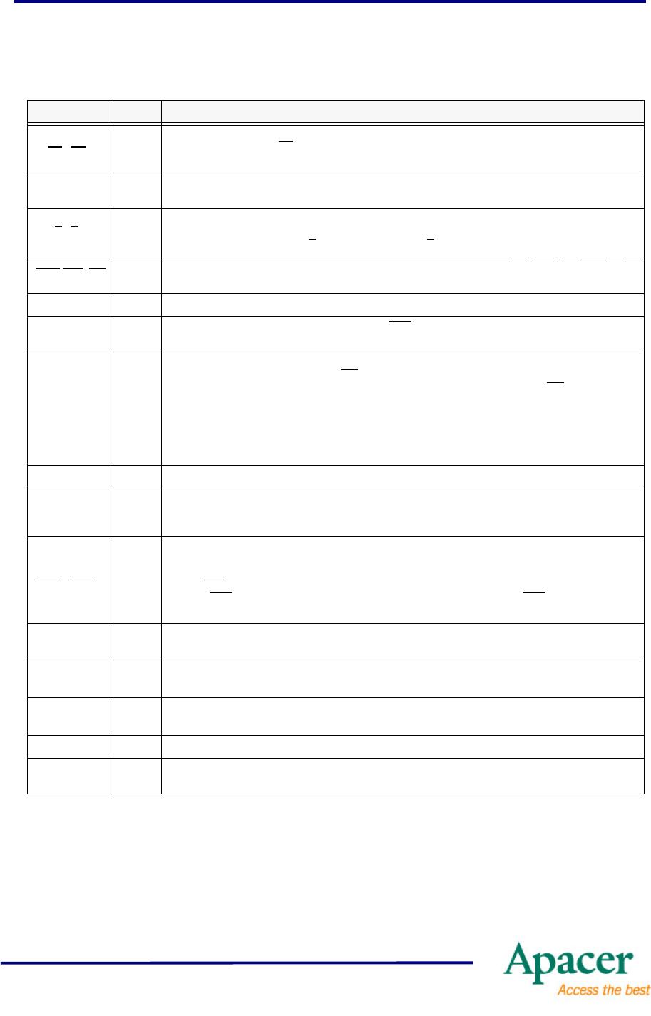
Input/Output Functional Description
Symbol Type Function
CK0-CK1
CK
0-CK1
Input
The system clock inputs. All address and command lines are sampled on the cross point of the rising edge
of CK and falling edge of CK . A Delay Locked Loop (DLL) circuit is driven from the clock input and output
timing for read operations is synchronized to the input clock.
CKE0-CKE1 Input
Activates the DDR2 SDRAM CK signal when high and deactivates the CK signal when low, By deactivat-
ing the clocks, CKE low initiates the Power Down mode or the Self Refesh mode.
S
0-S1 Input
Enables the associated DDR2 SDRAM command decoder when low and disables the command decoder
when high. When the command decoder is disabled, new commands are ignored but previous operations
continue. Rank 0 is selected by S
0, Rank 1 is selected by S1. Ranks are also called “Physical banks”.
RAS
, CAS, WE Input
When sampled at the cross point of the rising edge of CK and falling edge of CK, CAS, RAS, and WE
define the operation to be executed by the SDRAM.
BA0~BA2 Input Selects which DDR2 SDRAM internal bank is activated.
ODT0~ODT1 Input
Asserts on-die termination for DQ, DM, DQS, and DQS
signals if enabled via the DDR2 SDRAM Extended
Mode Register Set (EMRS).
A0~A9,
A10/AP,
A11~A13
Input
During a Bank Activate command cycle, defines the row address when sampled at the cross point of the
rising edge of CK and falling edge of CK.
During a Read or Write command cycle, defines the column
address when sampled at the cross point of the rising edge of CK and falling edge of CK. In addition to the
column address, AP is used to invoke autoprecharge operation at the end of the burst read or write cycle.
If AP is high, autoprecharge is selected and BA0-BAn defines the bank to be precharged. If AP is low,
autoprecharge is disabled. During a Precharge command cycle, AP is used in conjunction with BA0-BAn
to control which bank(s) to precharge. If AP is high, all banks will be pecharged regardiess of the state of
BA0-BAn inputs. If AP is low, then BA0-BAn are used to define which bank to precharge.
DQ0~DQ63 In/Out Data Input/Output pins.
DM0~DM7 Input
The data write masks, associated with one data byte. In Write mode, DM operates as a byte
mask by allowing input data to be written if it is low but blocks the write operation if it is high. In
Read mode, DM lines have no effect.
DQS0~DQS7
DQS
0~DQS7
In/Out
The data strobes, associated with one data byte, sourced with data transfers. In Write mode,
the data strobe is sourced by the controller and is centered in the data window. In Read mode,
the data strobe is sourced by the DDR2 SDRAMs and is sent at the leading edge of the data
window. DQS signals are complements, and timing is relative to the crosspoint of respective
DQS and DQS If the module is to be operated in single ended strobe mode, all DQS signals
must be tied on the system board to VSS and DDR2 SDRAM mode registers programmed appropriately.
V
DD
,V
DD
SPD,V
SS
Supply Power supplies for core, I/O, Serial Presence Detect, and ground for the module.
SDA In/Out
This is a bidirectional pin used to transfer data into or out of the SPD EEPROM. A resistor must be con-
nected to V
DD
to act as a pull up.
SCL Input
This signal is used to clock data into and out of the SPD EEPROM. A resistor may be connected from SCL
to V
DD
to act as a pull up.
SA0~SA1 Input Address pins used to select the Serial Presence Detect base address.
TEST In/Out
The TEST pin is reserved for bus analysis tools and is not connected on normal memory modules(SO-
DIMMs).
96SD2-1G800NN-AP3

Mfr. #:
Manufacturer:
Advantech
Description:
Memory Modules 1G SO-DDR2-800 200PIN 128X8 SAM(G)
Lifecycle:
New from this manufacturer.
Delivery:
DHL FedEx Ups TNT EMS
Payment:
T/T Paypal Visa MoneyGram Western Union

Products related to this Datasheet