23
LTC1197/LTC1197L
LTC1199/LTC1199L
Interfacing to the Parallel Port of the
Intel 8051 Family
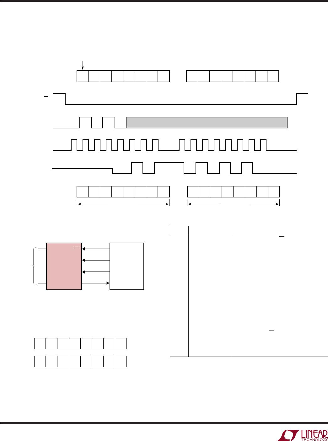
The Intel 8051 has been chosen to demonstrate the
interface between the LTC1199 and parallel port micro-
processors. Normally, the CS, CLK and D
IN
signals would
be generated on three port lines and the D
OUT
signal read
on a fourth port line. This works very well. However, we
will demonstrate here an interface with the D
IN
and D
OUT
of the LTC1199 tied together as described in the
SERIAL INTERFACE section. This saves one wire.
The 8051 first sends the start bit and MUX address to the
LTC1199 over the data line connected to P1.2. Then P1.2
is reconfigured as an input (by writing to it a one) and
the 8051 reads back the 8-bit A/D result over the same
data line.
LABEL MNEMONIC OPERAND COMMENTS
MOV A, #FFH D
IN
word for LTC1199
SETB P1.4 Make sure CS is high
CLR P1.4 CS goes low
MOV R4, #04 Load counter
LOOP 1 RLC A Rotate D
IN
bit into Carry
CLR P1.3 CLK goes low
MOV P1.2, C Output D
IN
bit into Carry
SETB P1.3 CLK goes high
DJNZ R4, LOOP 1 Next bit
MOV P1, #04 Bit 2 becomes an input
CLR P1.3 CLK goes low
MOV R4, #0AH Load counter
LOOP MOV C, P1.2 Read data bit into Carry
RLC A Rotate data bit into ACC
SETB P1.3 CLK goes high
CLR P1.3 CLK goes low
DJNZ R4, LOOP Next bit
MOV R2, A Store MSBs in R2
MOV C, P1.2 Read data bit into Carry
SETB P1.3 CLK goes high
CLR P1.3 CLK goes low
CLR A Clear ACC
RLC A Rotate data bit from Carry to
ACC
MOV C, P1.2 Read data bit into Carry
RRC A Rotate right into ACC
RRC A Rotate right into ACC
MOV R3, A Store LSBs in R3
SETB P1.4 CS goes high
D
OUT
from LTC1199 Stored in 8051 RAM
1
CS
CLK
DATA (D
IN
/D
OUT
)
START
ODD/
SIGN
DUMMY
B9
LTC1199 SENDS A/D RESULT
BACK TO 8051 P1.2
8051 P1.2 OUTPUTS DATA
TO LTC1199
8051 P1.2 RECONFIGURED
AS AN INPUT AFTER THE 4TH RISING
CLK AND BEFORE THE 4TH FALLING CLK
LTC1199 TAKES CONTROL OF DATA LINE
ON 4TH FALLING CLK
234
SGL/
DIFF
B8 B7 B6 B5 B4 B3 B2 B1 B0
1197/99 TA08
R2
1197/99 TA07
MSB
B9 B8 B7 B6 B5 B4 B3 B2
R3
LSB
B1 B0 0 0 0 0 0 0
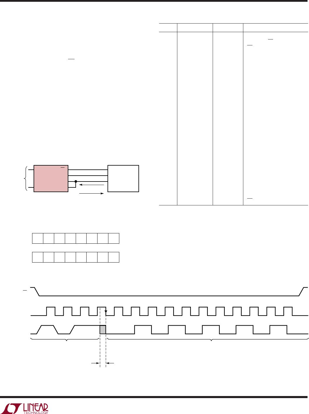
TYPICAL APPLICATIO S
U
CS
CLK
D
OUT
D
IN
LTC1199
ANALOG
INPUTS
P1.4
P1.3
P1.2
8051
MUX ADDRESS
A/D RESULT
1197/99 TA06