BD437TG

© Semiconductor Components Industries, LLC, 2013
December, 2013 − Rev. 17
1 Publication Order Number:
BD437/D
BD435G, BD437G, BD439G,
BD441G
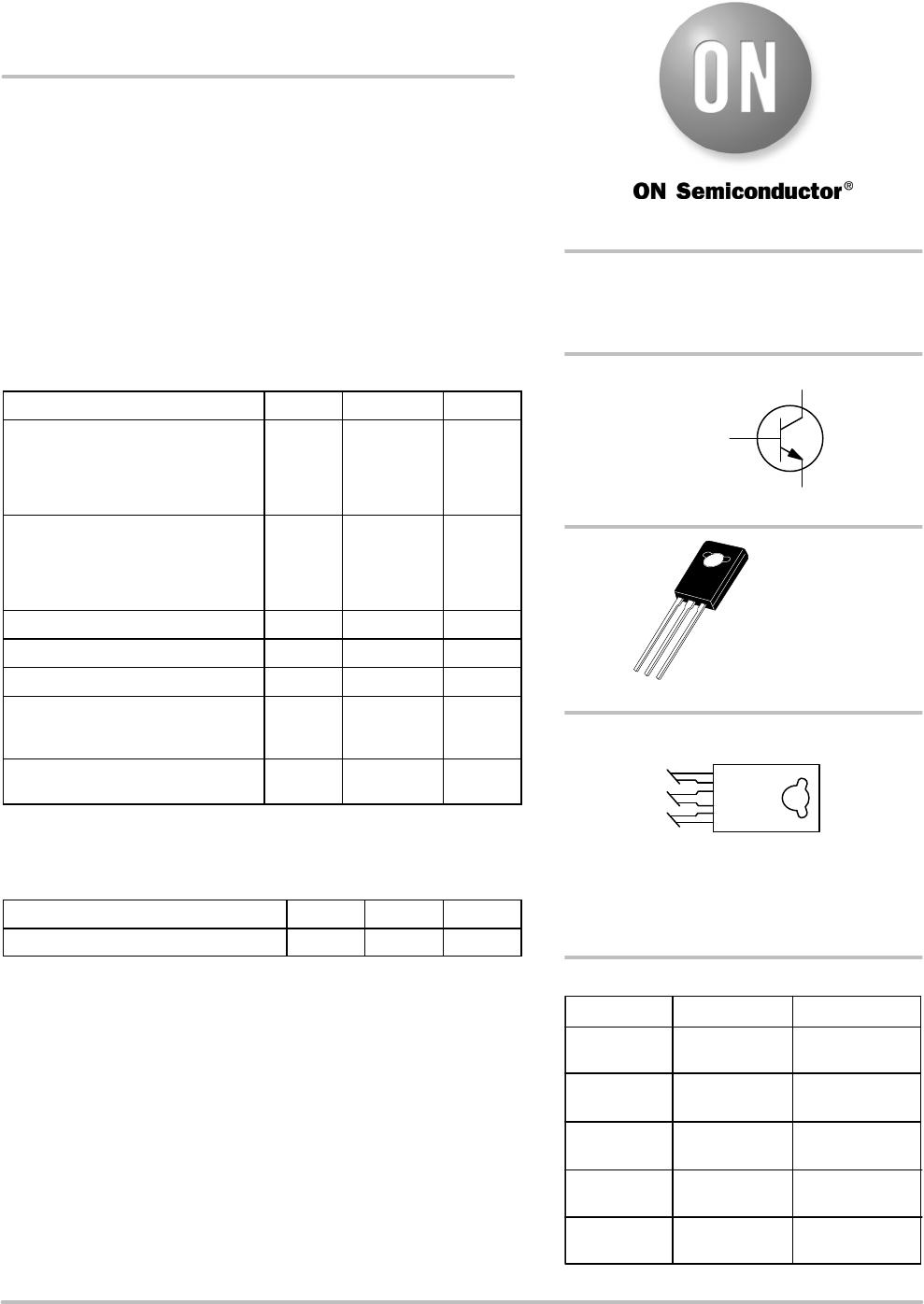
Plastic Medium-Power
Silicon NPN Transistors
This series of plastic, medium−power silicon NPN transistors can be
used for amplifier and switching applications.
Features
Complementary Types are BD438 and BD442
These Devices are Pb−Free and are RoHS Compliant*
MAXIMUM RATINGS
Rating Symbol Value Unit
Collector−Emitter Voltage
BD435G
BD437G
BD439G
BD441G
V
CEO
32
45
60
80
Vdc
Collector−Base Voltage
BD435G
BD437G
BD439G
BD441G
V
CBO
32
45
60
80
Vdc
Emitter−Base Voltage V
EBO
5.0 Vdc
Collector Current I
C
4.0 Adc
Base Current I
B
1.0 Adc
Total Device Dissipation
@ T
C
= 25°C
Derate above 25°C
P
D
36
288
W
W/°C
Operating and Storage Junction
Temperature Range
T
J
, T
stg
55 to +150 °C
Stresses exceeding those listed in the Maximum Ratings table may damage the
device. If any of these limits are exceeded, device functionality should not be
assumed, damage may occur and reliability may be affected.
THERMAL CHARACTERISTICS
Characteristic Symbol Max Unit
Thermal Resistance, Junction−to−Case
R
q
JC
3.5 °C/W
*For additional information on our Pb−Free strategy and soldering details, please
download the ON Semiconductor Soldering and Mounting Techniques
Reference Manual, SOLDERRM/D.
http://onsemi.com
Device Package Shipping
4.0 AMPERES
POWER TRANSISTORS
NPN SILICON
MARKING DIAGRAM
ORDERING INFORMATION
Y = Year
WW = Work Week
BD4xx = Device Code
xx = 35, 37, 37T, 39, 41
G = Pb−Free Package
BD435G TO−225
(Pb−Free)
500 Units/Box
BD437G TO−225
(Pb−Free)
500 Units/Box
BD437TG TO−225
(Pb−Free)
50 Units/Rail
BD439G TO−225
(Pb−Free)
500 Units/Box
BD441G TO−225
(Pb−Free)
500 Units/Box
BASE 3
EMITTER 1
COLLECTOR 2, 4
TO−225
CASE 77−09
STYLE 1
1
2
3
YWW
BD4xxG
BD435G, BD437G, BD439G, BD441G
http://onsemi.com
2
ELECTRICAL CHARACTERISTICS (T
C
= 25°C unless otherwise noted)
Characteristic
Symbol Min Typ Max Unit
Collector−Emitter Breakdown Voltage
(I
C
= 100 mA, I
B
= 0)
BD435G
BD437G
BD439G
BD441G
V
(BR)CEO
32
45
60
80
Vdc
Collector−Base Breakdown Voltage
(I
C
= 100 mA, I
B
= 0)
BD435G
BD437G
BD439G
BD441G
V
(BR)CBO
32
45
60
80
Vdc
Emitter−Base Breakdown Voltage
(I
E
= 100 mA, I
C
= 0)
V
(BR)EBO
5.0
Vdc
Collector Cutoff Current
(V
CB
= 32 V, I
E
= 0)
BD435G
(V
CB
= 45 V, I
E
= 0)
BD437G
(V
CB
= 60 V, I
E
= 0)
BD439G
(V
CB
= 80 V, I
E
= 0)
BD441G
I
CBO
0.1
0.1
0.1
0.1
mAdc
Emitter Cutoff Current
(V
EB
= 5.0 V)
I
EBO
1.0
mAdc
DC Current Gain
(I
C
= 10 mA, V
CE
= 5.0 V)
BD435G
BD437G
BD439G
BD441G
h
FE
40
30
20
15
DC Current Gain
(I
C
= 500 mA, V
CE
= 1.0 V)
BD435G
BD437G
BD439G, BD441G
h
FE
85
85
40
475
375
475
DC Current Gain
(I
C
= 2.0 A, V
CE
= 1.0 V)
BD435G
BD437G
BD439G
BD441G
h
FE
50
40
25
15
Collector Saturation Voltage
(I
C
= 2.0 A, I
B
= 0.2 V)
BD435G
(I
C
= 3.0 A, I
B
= 0.3 A)
BD437G, BD439G, BD441G
V
CE(sat)
0.5
0.8
Vdc
Base−Emitter On Voltage
(I
C
= 2.0 A, V
CE
= 1.0 V)
V
BE(on)
1.1
Vdc
Current−Gain − Bandwidth Product
(V
CE
= 1.0 V, I
C
= 250 mA, f = 1.0 MHz)
f
T
3.0
MHz
Product parametric performance is indicated in the Electrical Characteristics for the listed test conditions, unless otherwise noted. Product
performance may not be indicated by the Electrical Characteristics if operated under different conditions.
BD435G, BD437G, BD439G, BD441G
http://onsemi.com
3
V
CE
, COLLECTOR−EMITTER VOLTAGE (VOLTS)
Figure 1. Collector Saturation Region
I
B
, BASE CURRENT (mA)
2.0
0
0.05
1.6
1.2
0.8
0.4
1.0 2.0 10 70 500
I
C
= 10 A 100 mA 1.0 A
0.1 100205.0
T
J
= 25°C
3.0 300.07 300200507.00.2 0.3 0.5 0.7
3.0 A
Figure 2. Current Gain
200
0
0.01
180
160
80
0.1
BD439, 441
0.02 30.30.2 1 520.50.03 0.05
I
C
, COLLECTOR CURRENT (AMP)
h
FE
, CURRENT GAIN (NORMALIZED)
BD433, 435, 437
140
120
100
60
40
20
2.0
0.005
I
C
, COLLECTOR CURRENT (AMP)
1.6
1.2
0.8
0.6
0
T
J
= 25°C
V
BE(sat)
@ I
C
/I
B
= 10
V
CE(sat)
@ I
C
/I
B
= 10
VOLTAGE (VOLTS)
Figure 3. “On” Voltage
0.02 0.030.05 0.1 0.2
V
BE
@ V
CE
= 2.0 V
0.01 0.3 0.5 1.0 2.0 3.0 4.
0
Figure 4. Active Region Safe Operating Area
10
V
CE
, COLLECTOR−EMITTER VOLTAGE (VOLTS)
4.0
1.0
0.1
2.0 10 20 100
0.5
I
C
, COLLECTOR CURRENT (AMP)
T
J
= 150°C
dc
5 ms
1.0 5.0 50
SECONDARY BREAKDOWN
THERMAL LIMIT T
C
= 25°C
BONDING WIRE LIMIT
CURVES APPLY BELOW RATED V
CEO
BD437
BD439
BD441

BD437TG

Mfr. #:
Manufacturer:
ON Semiconductor
Description:
Bipolar Transistors - BJT 4A 45V 36W NPN
Lifecycle:
New from this manufacturer.
Delivery:
DHL FedEx Ups TNT EMS
Payment:
T/T Paypal Visa MoneyGram Western Union

Products related to this Datasheet