342MPLFT

ICS342
FIELD PROGRAMMABLE DUAL OUTPUT SS VERSACLOCK SYNTHESIZER EPROM CLOCK SYNTHESIZER
IDT® / ICS™
FIELD PROGRAMMABLE DUAL OUTPUT SS VERSACLOCK SYNTHESIZER 4
ICS342 REV N 090613
Absolute Maximum Ratings
Stresses above the ratings listed below can cause permanent damage to the ICS342. These ratings, which are
standard values for IDT commercially rated parts, are stress ratings only. Functional operation of the device at these
or any other conditions above those indicated in the operational sections of the specifications is not implied.
Exposure to absolute maximum rating conditions for extended periods can affect product reliability. Electrical
parameters are guaranteed only over the recommended operating temperature range.
Recommended Operation Conditions
Parameter Condition Min. Typ. Max. Units
Supply Voltage, VDD Referenced to GND 7 V
Inputs Referenced to GND -0.5 VDD+ 0.5 V
Clock Outputs Referenced to GND -0.5 VDD+ 0.5 V
Storage Temperature -65 150 C
Soldering Temperature Max 10 seconds 260 C
Junction Temperature 125 C
Parameter Min. Typ. Max. Units
Ambient Operating Temperature (ICS342M) 0 +70 C
Ambient Operating Temperature (ICS342MI) -40 +85 C
Power Supply Voltage (measured in respect to GND) +3.15 +3.3 +3.45 V
Power Supply Ramp Time 4 ms
ICS342
FIELD PROGRAMMABLE DUAL OUTPUT SS VERSACLOCK SYNTHESIZER EPROM CLOCK SYNTHESIZER
IDT® / ICS™
FIELD PROGRAMMABLE DUAL OUTPUT SS VERSACLOCK SYNTHESIZER 5
ICS342 REV N 090613
DC Electrical Characteristics
Unless stated otherwise, VDD = 3.3V ±5%, Ambient Temperature -40 to +85C
Note 1: Example with 25 MHz crystal input with two outputs of 33.3
MHz, no load, and VDD = 3.3 V.
Parameter Symbol Conditions Min. Typ. Max. Units
Operating Voltage VDD 3.15 3.3 3.45 V
Operating Supply Current
Input High Voltage
IDD
Configuration
Dependent - See
VersaClock
TM
Estimates
mA
Two 33.3333 MHz
outputs, PDTS
= 1, no
load, Note 1
13 mA
PDTS
= 0 20 A
Input High Voltage V
IH
SEL pin 2 V
Input Low Voltage V
IL
SEL pin 0.4 V
Input High Voltage, PDTS
V
IH
VDD-0.5 V
Input Low Voltage, PDTS
V
IL
0.4 V
Input High Voltage V
IH
ICLK VDD/2+1 V
Input Low Voltage V
IL
ICLK VDD/2-1 V
Output High Voltage
(CMOS High)
V
OH
I
OH
= -4 mA VDD-0.4 V
Output High Voltage V
OH
I
OH
= -12 mA 2.4 V
Output Low Voltage V
OL
I
OL
= 12mA 0.4 V
Short Circuit Current I
OS
±70 mA
Nominal Output
Impedance
Z
O
20
Internal pull-up resistor R
PUP
SEL, PDTS pins 250 k
Internal pull-down
resistor
R
PD
CLK output 525 k
Input Capacitance C
IN
Inputs 4 pF
ICS342
FIELD PROGRAMMABLE DUAL OUTPUT SS VERSACLOCK SYNTHESIZER EPROM CLOCK SYNTHESIZER
IDT® / ICS™
FIELD PROGRAMMABLE DUAL OUTPUT SS VERSACLOCK SYNTHESIZER 6
ICS342 REV N 090613
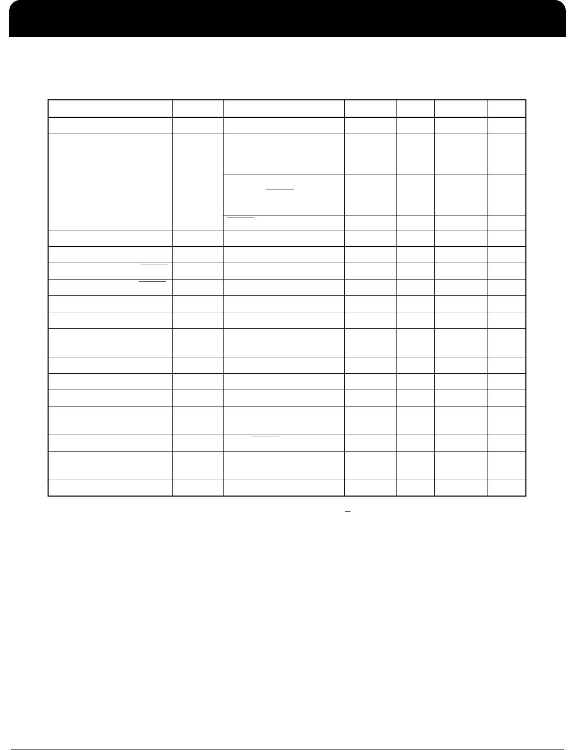
AC Electrical Characteristics
Unless stated otherwise, VDD = 3.3V ±5%, Ambient Temperature -40 to +85 C
Note 1: Measured with 15 pF load.
Note 2: Duty Cycle is configuration dependent. Most configurations are minimum 45% and maximum 55%.
Note 3: IDT test mode output occurs for first 170 clock cycles on CLK2 for each PLL powered up. PDTS
transition
high on select address change.
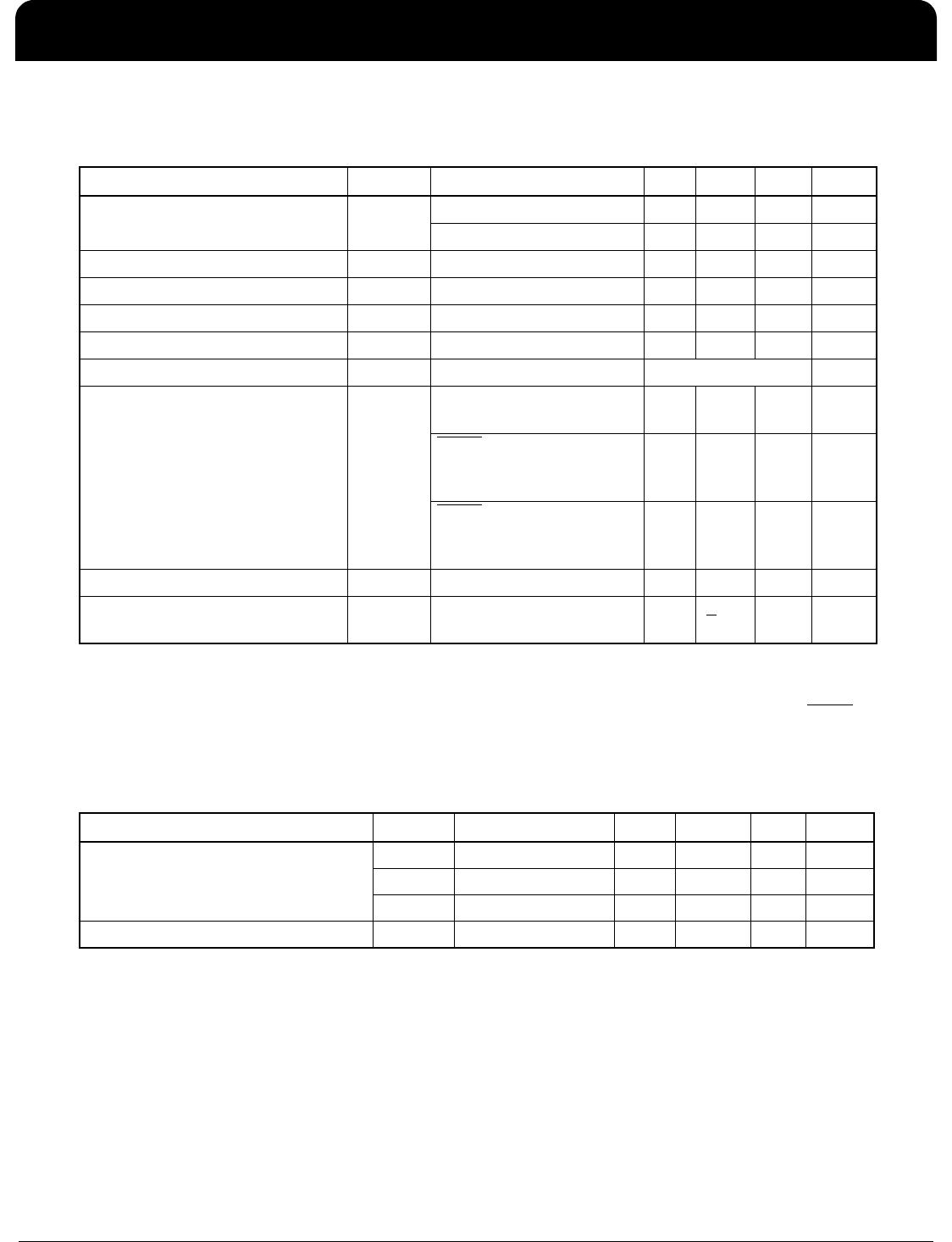
Thermal Characteristics
Parameter Symbol Conditions Min. Typ. Max. Units
Input Frequency F
IN
Fundamental Crystal 5 27 MHz
Input Clock 2 50 MHz
Output Frequency 0.25 200 MHz
Output Rise Time t
OR
20% to 80%, Note 1 1 ns
Output Fall Time t
OF
80% to 20%, Note 1 1 ns
Duty Cycle Note 2 40 49-51 60 %
Output Frequency Synthesis Error Configuration Dependent TBD ppm
Power-up time PLL lock time from
power-up, Note 3
410ms
PDTS
goes high until
stable CLK output, Spread
Spectrum Off, Note 3
0.2 2 ms
PDTS
goes high until
stable CLK output, Spread
Spectrum On, Note 3
47ms
One Sigma Clock Period Jitter Configuration Dependent 50 ps
Maximum Absolute Jitter t
ja
Deviation from Mean.
Configuration Dependent
+200 ps
Parameter Symbol Conditions Min. Typ. Max. Units
Thermal Resistance Junction to
Ambient
JA
Still air 150 C/W
JA
1 m/s air flow 140 C/W
JA
3 m/s air flow 120 C/W
Thermal Resistance Junction to Case
JC
40 C/W

342MPLFT

Mfr. #:
Manufacturer:
IDT
Description:
Clock Synthesizer / Jitter Cleaner VERSACLOCK SYNTHESIZER
Lifecycle:
New from this manufacturer.
Delivery:
DHL FedEx Ups TNT EMS
Payment:
T/T Paypal Visa MoneyGram Western Union

Products related to this Datasheet