4
ICS9112-17
0051K—11/02/04
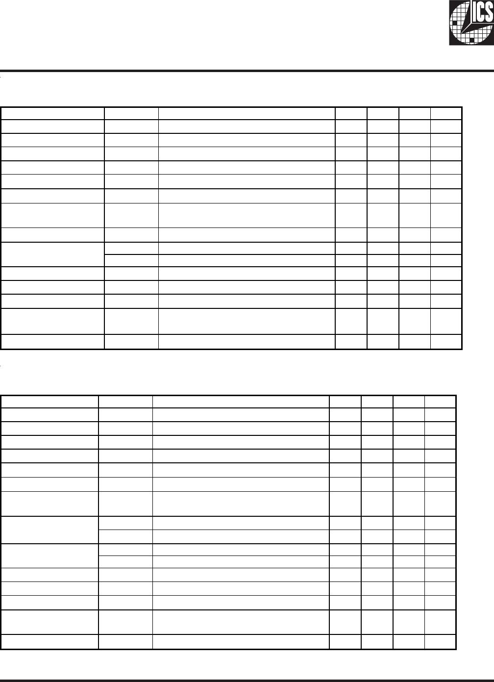
Electrical Characteristics - OUTPUT
T
A
= 0 - 70°C; V
DD
= V
DDL
= 3.3 V +/-10%; C
L
= 20 - 30 pF (unless otherwise stated)
PARAMETER SYMBOL CONDITIONS MIN TYP MAX UNITS
Output Impedance R
DSP
V
O
= V
D
*(0.5) 10 24
Ω
Output Impedance R
DSN
V
O
= V
D
*(0.5) 10 24
Ω
Output High Voltage V
OH
I
OH
= -8 mA 2.4 2.9 3.3 V
Output Low Voltage V
OL
I
OL
= 8 mA 0.25 0.4 V
Rise Time
1
T
r
V
OL
= 0.8 V, V
OH
= 2.0 V 1.2 2.0 ns
Fall Time
1
T
f
V
OH
= 2.0 V, V
OL
= 0.8 V 1.2 2.0 ns
PLL Lock Time1 tLOCK
Stable power supply, valid clock
presented on REF pin
1.0 ms
D
t
V
= 1.4V;Cl=30pF 40 50 60 %
D
t
V
= Vdd/2; Fout <66.6MHz 45 50 55 %
Tcyc-cyc at 66MHz , Loaded Outputs 250 ps
Tcyc-cyc >66MHz , Loaded Outputs 200 ps
Absolute Jitter
1
Tjabs 10000 cycles; Cl=30pF -100 70 100 ps
Jitter; 1-Sigma
1
Tj1s 10000 cycles; Cl=30pF 14 30 ps
Skew
1
T
sk
V
= 1.4 V (Window) Output to Output 250 ps
evice to Device Ske
Tdsk-Tdsk
Measured at VDD/2 on the CLKOUT
pins of devices
0700ps
Delay Input-Output
1
D
R1
V
T
= 1.4 V
0700ps
1
Guaranteed by design, not 100% tested in production.
Cycle to Cycle jitter
1
Duty Cycle
1
Electrical Characteristics - OUTPUT
T
A
= 0 - 70°C; V
DD
= V
DDL
= 5.0 V +/-10%; C
L
= 20 - 30 pF (unless otherwise stated)
PARAMETER SYMBOL CONDITIONS MIN TYP MAX UNITS
Output Impedance R
DSP
V
O
= V
DD
*(0.5) 10 24
Ω
Output Impedance R
DSN
V
O
= V
DD
*(0.5) 10 24
Ω
Output High Voltage V
OH
I
OH
= -8 mA 2.4 2.9 5.0 V
Output Low Voltage V
OL
I
OL
= 8 mA 0.25 0.4 V
Rise Time
1
T
r
V
OL
= 0.8 V, V
OH
= 2.0 V 0.8 1.5 ns
Fall Time
1
T
f
V
OH
= 2.0 V, V
OL
= 0.8 V 1.0 1.5 ns
PLL Lock Time
1
tLOCK
Stable power supply, valid clock
presented on REF pin
1.0 ms
Duty Cycle
1
D
t
V
= 1.4V;Cl=30pF 40 50 60 %
Tcyc-cyc at 66MHz , Loaded Outputs 250 ps
Tcyc-cyc >66MHz , Loaded Outputs 200 ps
Absolute Jitter
1
Tjabs 10000 cycles; Cl=30pF -100 60 100 ps
Jitter; 1-Si
ma
1
Tj1s 10000 c
cles; Cl=30pF 14 30 ps
Skew
1
T
sk
V
= 1.4 V (Window) Output to Output 250 ps
Device to Device
Skew
1
Tdsk-Tdsk
Measured at VDD/2 on the CLKOUT
pins of devices
0 700 ps
Delay Input-Output
1
D
R1
V
T
= 1.4 V
0 700 ps
1
Guaranteed by design, not 100% tested in production.
Cycle to Cycle jitter
1

