CBTD16210DGG,518

Philips Semiconductors Product specification
CBTD16210
20-bit level shifting bus switch
with 10-bit output enables
2000 Oct 12
3
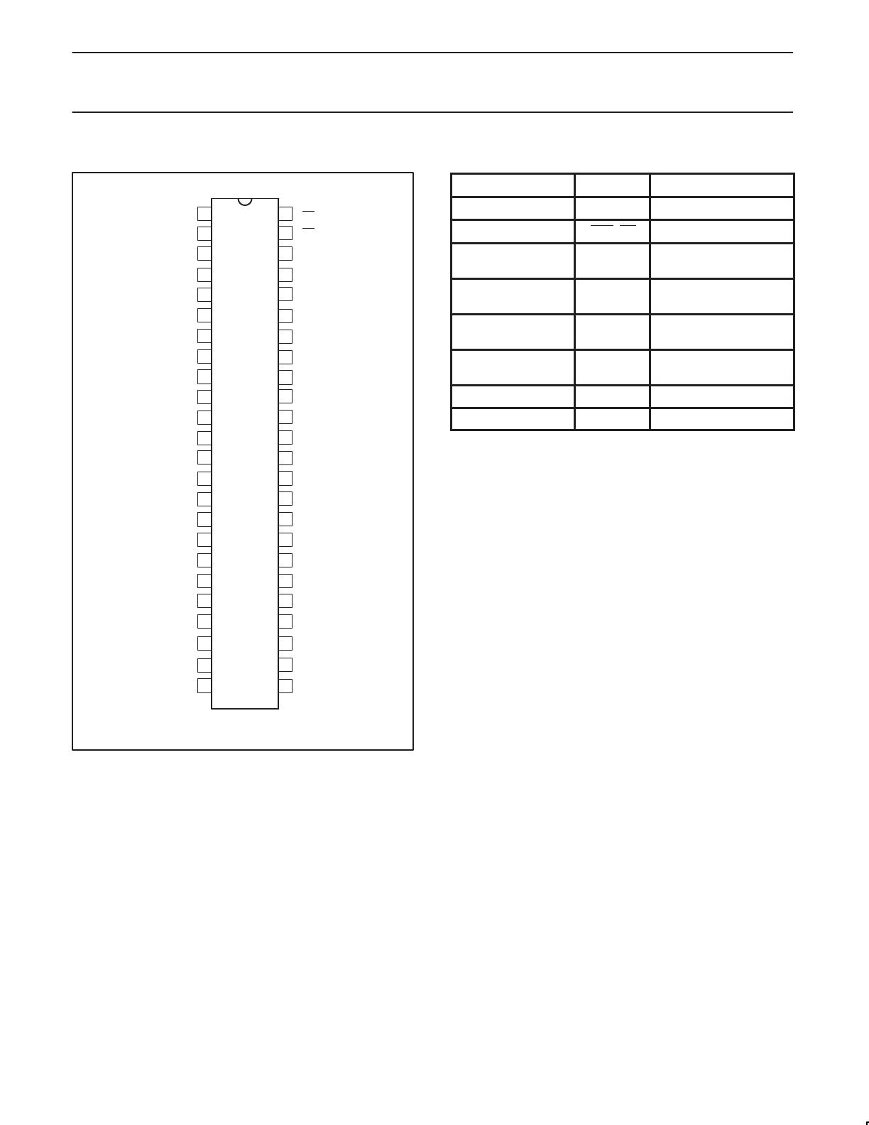
PIN CONFIGURATION
1
2
3
4
5
6
7
8
9
10
11
12
13
14
15
16
17
18
19
20
25
26
27
28
29
30
31
32
33
34
35
36
37
38
39
40
21
22
23
24
41
42
43
44
45
46
47
48
NC
1A1
1A2
1A3
1A4
1A5
1A6
GND
1A7
1A8
1A9
1A10
2A1
2A2
V
CC
2A3
GND
2A4
2A5
2A6
2A7
2A8
2A9
2A10
1OE
2OE
1B1
1B2
1B3
1B4
1B5
GND
1B6
1B7
1B8
1B9
1B10
2B1
2B2
2B3
GND
2B4
2B5
2B6
2B7
2B8
2B9
2B10
SA00546
PIN DESCRIPTION
PIN NUMBER SYMBOL NAME AND FUNCTION
1 NC No internal connection
48, 47 1OE, 2OE Output enables
2, 3, 4, 5, 6, 7, 9, 10,
11, 12
1A1-1A10 Inputs
46, 45, 44, 43, 42, 40,
39, 38, 37, 36
1B1-1B10 Outputs
13, 14, 16, 18, 19, 20,
21, 22, 23, 24
2A1-2A10 Inputs
35, 34, 33, 31, 30, 29,
28, 27, 26, 25
2B1-2B10 Outputs
8, 17, 32, 41 GND Ground (0V)
15 V
CC
Positive supply voltage
Philips Semiconductors Product specification
CBTD16210
20-bit level shifting bus switch
with 10-bit output enables
2000 Oct 12
4
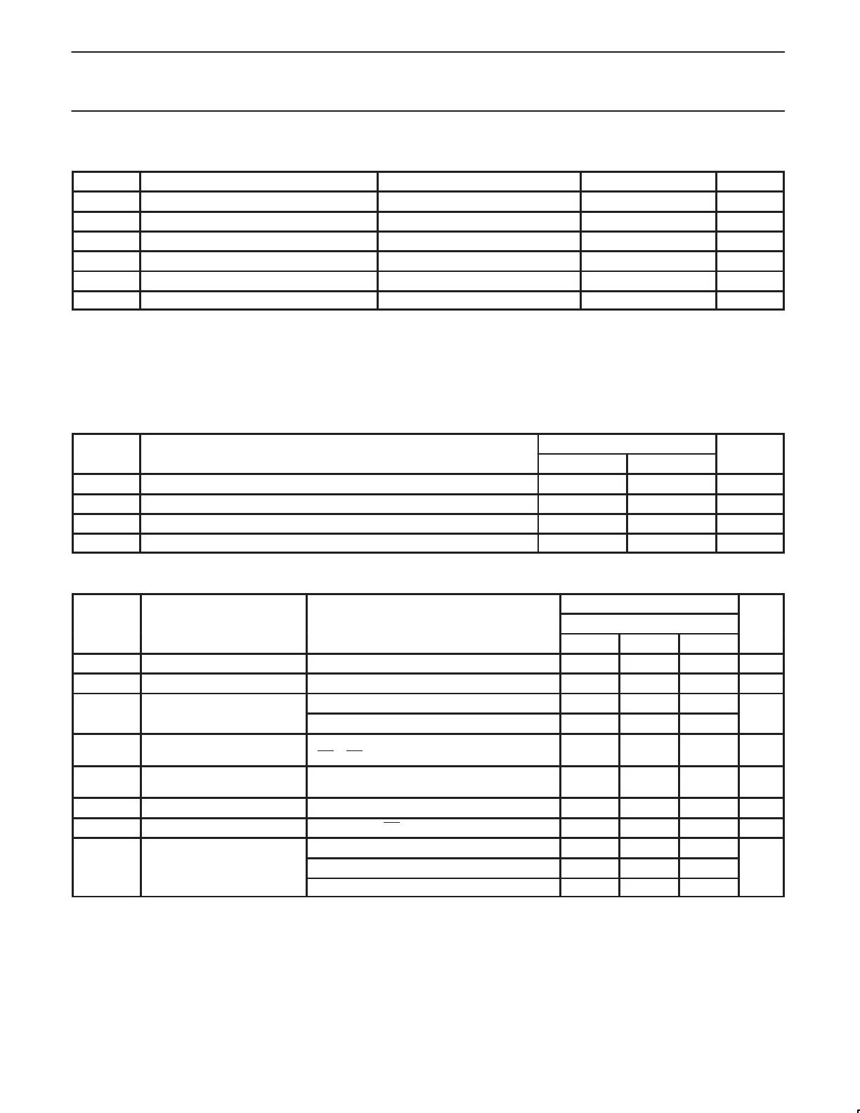
ABSOLUTE MAXIMUM RATINGS
1,
2
SYMBOL
PARAMETER CONDITIONS RATING UNIT
V
CC
DC supply voltage –0.5 to +7.0 V
I
IK
DC input diode current V
I
< 0 –50 mA
V
I
DC input voltage
3
–0.5 to +7.0 V
V
OUT
DC output voltage
3
output in Off or High state –0.5 to +5.5 V
I
OUT
DC output current output in Low state 128 mA
T
stg
Storage temperature range –65 to +150 °C
NOTES:
1. Stresses beyond those listed may cause permanent damage to the device. These are stress ratings only and functional operation of the
device at these or any other conditions beyond those indicated under “recommended operating conditions” is not implied. Exposure to
absolute-maximum-rated conditions for extended periods may affect device reliability.
2. The performance capability of a high-performance integrated circuit in conjunction with its thermal environment can create junction
temperatures which are detrimental to reliability. The maximum junction temperature of this integrated circuit should not exceed 150°C.
3. The input and output voltage ratings may be exceeded if the input and output current ratings are observed.
RECOMMENDED OPERATING CONDITIONS
SYMBOL
PARAMETER
LIMITS
UNIT
SYMBOL
PARAMETER
Min Max
UNIT
V
CC
DC supply voltage 4.5 5.5 V
V
IH
High-level input voltage 2.0 V
V
IL
Low-level Input voltage 0.8 V
T
amb
Operating free-air temperature range –40 +85 °C
DC ELECTRICAL CHARACTERISTICS
LIMITS
SYMBOL PARAMETER TEST CONDITIONS T
amb
= –40°C to +85°C UNIT
Min Typ
1
Max
V
IK
Input clamp voltage V
CC
= 4.5 V; I
I
= –18 mA –1.2 V
V
OH
Output high pass voltage See Figure 1, page 6 V
I
In
p
ut leakage current
V
CC
= 0 V; V
I
= 5.5 V 10
µA
I
I
Inp
u
t
leakage
c
u
rrent
V
CC
= 5.5 V; V
I
= GND or 5.5 V ±1
µ
A
I
CC
Quiescent supply current
2
V
CC
= 5.5 V; I
O
= 0, V
I
= V
CC
or GND;
1OE=2OE=GND
1.5 mA
I
CC
Additional supply current per
input pin
2
V
CC
= 5.5 V, one input at 3.4 V,
other inputs at V
CC
or GND
2.5 mA
C
I
Control pins V
I
= 3 V or 0 4.5 pF
C
IO(OFF)
Power-off leakage current V
O
= 3 V or 0, OE = V
CC
8 pF
3
V
CC
= 4.5 V; V
1
= 0 V; I
I
= 64 mA 5 7
r
on
3
V
CC
= 4.5 V; V
1
= 0 V; I
I
= 30 mA 5 7
V
CC
= 4.5 V; V
1
= 2.4 V; I
I
= –15 mA 16 50
NOTES:
1. All typical values are at V
CC
= 5 V, T
amb
= 25°C
2. This is the increase in supply current for each input that is at the specified TTL voltage level rather than V
CC
or GND
3. Measured by the voltage drop between the A and the B terminals at the indicated current through the switch.
On-state resistance is determined by the lowest voltage of the two (A or B) terminals.
Philips Semiconductors Product specification
CBTD16210
20-bit level shifting bus switch
with 10-bit output enables
2000 Oct 12
5
AC CHARACTERISTICS
GND = 0 V; t
R;
C
L
= 50 pF
SYMBOL
PARAMETER DESCRIPTION
LIMITS
–40°C to +85°C V
CC
= 5 V ± 0.5 V
UNITS
Min Mean Max
t
pd
Propagation delay
1
250 ps
t
PZH
Output enable time to HIGH level 1.5 5.0 7.5 ns
t
PHZ
Output disable time from HIGH level 1.0 2.5 4.5 ns
t
PZL
Output enable time to LOW level 1.5 6.0 9.0 ns
t
PLZ
Output disable time from LOW level 1.5 3.5 6.0 ns
NOTES:
1. This parameter is warranted but not production tested. The propagation delay is based on the RC time constant of the typical on-state
resistance of the switch and a load capacitance of 50 pF, when driven by an ideal voltage source (zero output impedance).
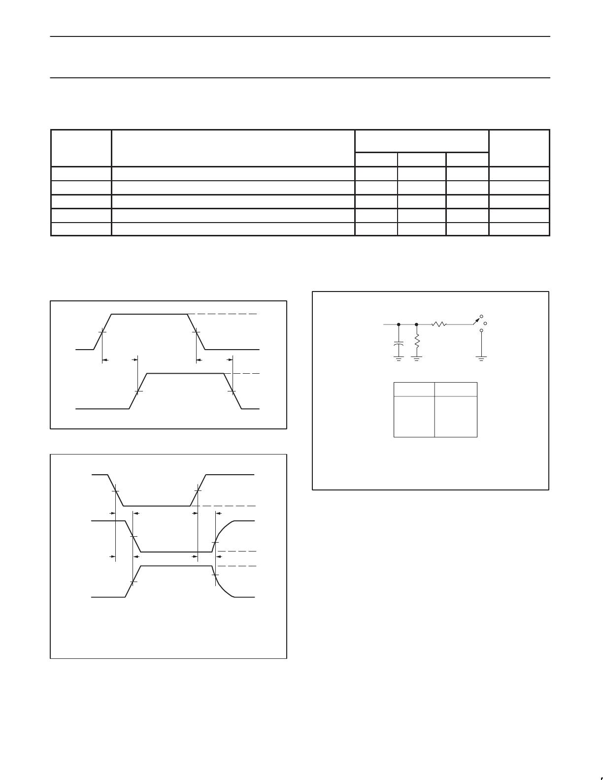
AC WAVEFORMS
V
M
= 1.5 V, V
IN
= GND to 3.0 V
INPUT
1.5V
OUTPUT
t
PLH
t
PHL
SA00028
1.5V
1.5V 1.5V
3 V
0 V
V
OH
V
OL
Waveform 1. Input (An) to Output (Yn) Propagation Delays
Output Control
(Low-level
enabling
1.5 V
t
PZH
t
PHZ
V
OH
V
OL
t
PZL
t
PLZ
3.5V
0V
V
OL
+ 0.3V
V
OH
– 0.3V
SA00029
1.5 V
1.5 V 1.5 V
0V
3V
Output
Waveform 1
S1 at 7 V
(see Note)
Note:
Waveform 1 is for an output with internal conditions such that
the output is low except when disabled by the output control.
Waveform 2 is for an output with internal conditions such that
the output is high except when disabled by the output control.
Output
Waveform 2
S1 at Open
(see Note)
Waveform 2. 3-State Output Enable and Disable Times
TEST CIRCUIT AND WAVEFORMS
C
L
= 50 pF
500
Load Circuit
DEFINITIONS
C
L
= Load capacitance includes jig and probe capacitance;
see AC CHARACTERISTICS for value.
TEST S1
t
pd
open
t
PLZ
/t
PZL
7 V
t
PHZ
/t
PZH
open
SA00012
500
From Output
Under Test
S1
7 V
Open
GND

CBTD16210DGG,518

Mfr. #:
Manufacturer:
Nexperia
Description:
IC 20-BIT BUS SW 48-TSSOP
Lifecycle:
New from this manufacturer.
Delivery:
DHL FedEx Ups TNT EMS
Payment:
T/T Paypal Visa MoneyGram Western Union