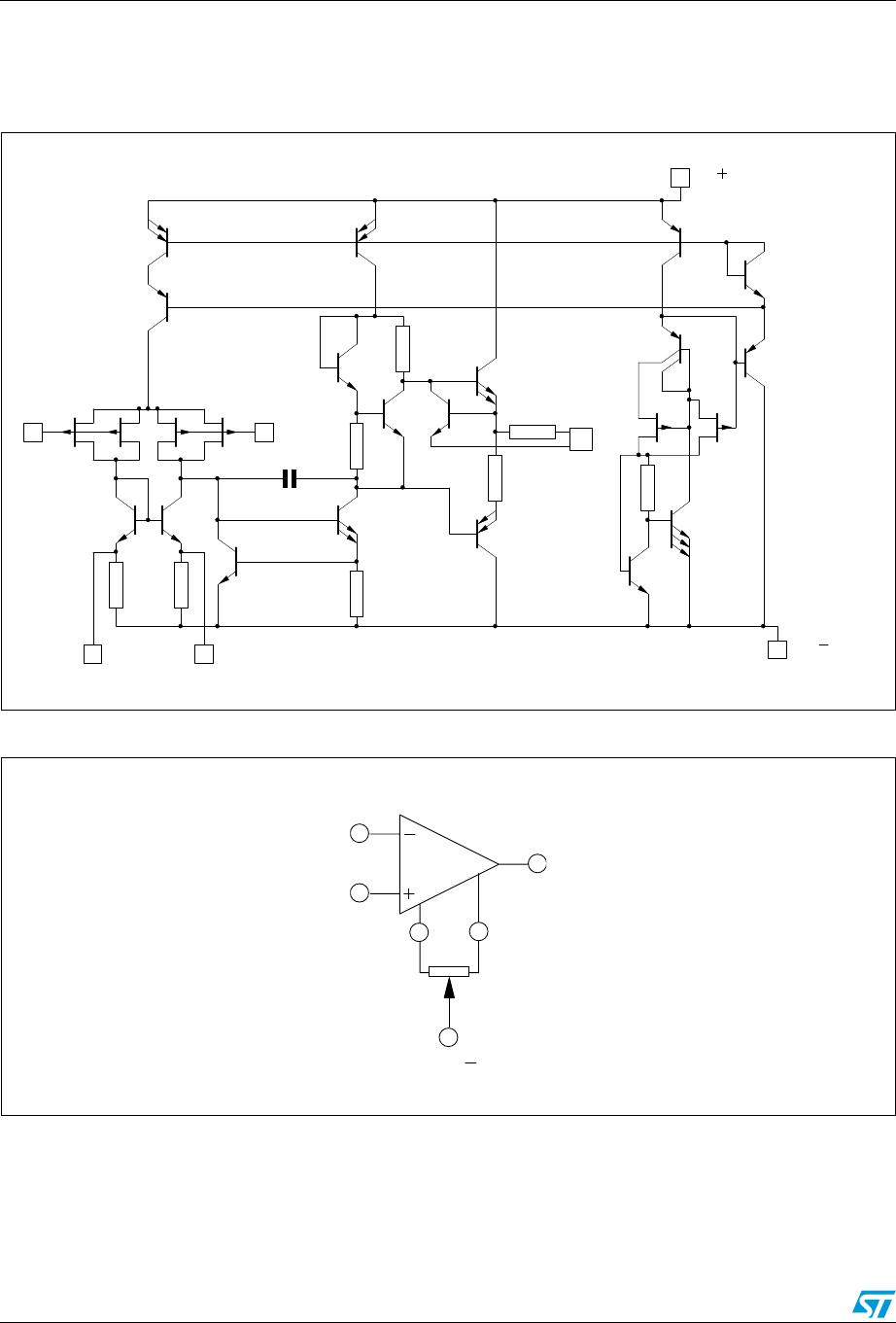
TL061 Absolute maximum ratings and operating conditions
3/16
2 Absolute maximum ratings and operating conditions
Table 1. Absolute maximum ratings
Symbol Parameter
Value
Unit
TL061M, AM, BM TL061I, AI, BI TL061C, AC, BC
V
CC
Supply voltage
(1)
±18 V
V
i
Input voltage
(2)
±15 V
V
id
Differential input voltage
(3)
±30 V
P
tot
Power dissipation 680 mW
Output short-circuit duration
(4)
Infinite
T
stg
Storage temperature range -65 to +150 -65 to +150 -65 to +150 °C
R
thja
Thermal resistance junction to
ambient
(5)
(6)
SO-8
DIP8
125
85
°C/W
R
thjc
Thermal resistance junction to
case
(5)
(6)
SO-8
DIP8
40
41
°C/W
ESD
HBM: human body model
(7)
800 V
MM: machine model
(8)
200 V
CDM: charged device model
(9)
1.5 kV
1. All voltage values, except differential voltage, are with respect to the zero reference level (ground) of the supply voltages
where the zero reference level is the midpoint between V
CC
+
and V
CC
-
.
2. The magnitude of the input voltage must never exceed the magnitude of the supply voltage or 15 volts, whichever is less.
3. Differential voltages are the non-inverting input terminal with respect to the inverting input terminal.
4. The output may be shorted to ground or to either supply. Temperature and/or supply voltages must be limited to ensure
that the dissipation rating is not exceeded.
5. Short-circuits can cause excessive heating and destructive dissipation.
6. Rth are typical values.
7. Human body model: 100 pF discharged through a 1.5 kΩ resistor between two pins of the device, done for all couples of pin
combinations with other pins floating.
8. Machine model: a 200 pF cap is charged to the specified voltage, then discharged directly between two pins of the device
with no external series resistor (internal resistor < 5 Ω), done for all couples of pin combinations with other pins floating.
9. Charged device model: all pins plus package are charged together to the specified voltage and then discharged directly to
the ground.
Table 2. Operating conditions
Symbol Parameter TL061M, AM, BM TL061I, AI, BI TL061C, AC, BC Unit
V
CC
Supply voltage range 6 to 36 V
T
oper
Operating free-air temperature range -55 to +125 -40 to +105 0 to +70 °C


