LTC2756
7
2756fa
For more information www.linear.com/LTC2756
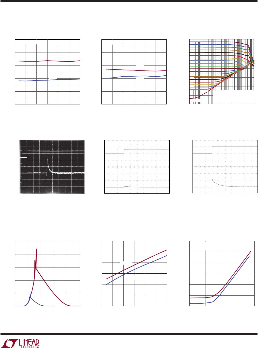
Typical perForMance characTerisTics
Settling Full-Scale Step
INL vs V
DD
DNL vs V
DD
Logic Threshold
vs Supply Voltage
Supply Current
vs Logic Input Voltage
Supply Current
vs Update Frequency
Mid-Scale Glitch (V
DD
= 3V)
DIGITAL INPUT VOLTAGE (V)
0
SUPPLY CURRENT (mA)
3
4
5
4
2756 G16
2
1
0
1
2
3
5
V
DD
= 5V
CLR, LDAC, SDI, SCK,
CS/LD TIED TOGETHER
V
DD
= 3V
V
DD
(V)
2.5
0.5
LOGIC THRESHOLD (V)
0.75
1
1.25
1.5
2
3
3.5 4 4.5
5 5.5
1.75
2756 G17
RISING
FALLING
SCK FREQUENCY (Hz)
1
0.0001
SUPPLY CURRENT (mA)
0.001
0.01
0.1
1
10
100
V
DD
= 5V
100 10k 1M 100M
2756 G18
V
DD
= 3V
ALTERNATING ZERO-SCALE
AND FULL-SCALE
500ns/DIV
CS/LD
5V/DIV
GATED
SETTLING
WAVEFORM
100µV/DIV
(AVERAGED)
2756 G13
LT1468 AMP; C
FEEDBACK
= 20pF
0V TO 10V STEP
V
REF
= –10V; SPAN CODE = 0000
t
SETTLE
= 1.8µs to 0.0004% (18 BITS)
V
DD
= 5V, V(R
IN
) = 5V, T
A
= 25°C, unless otherwise noted.
Mid-Scale Glitch (V
DD
= 5V)
Multiplying Frequency Response
vs Digital Code
ALL BITS ON
ALL BITS OFF
FREQUENCY (Hz)
100 1k 10k
–140
ATTENUATION (dB)
–100
–120
–60
–80
–40
–20
0
1M100k 10M
2756 G12
0V TO 5V OUTPUT RANGE
LT1468 OUTPUT AMPLIFIER
C
FEEDBACK
= 15pF
ALL BITS OFF
D17
D16
D15
D14
D13
D12
D11
D10
D9
D8
D7
D6
D5
D4
D3
D2
D1
D0
V
DD
(V)
2.5 3.5 4
–1.0
INL (LSB)
–0.8
–0.6
–0.2
–0.4
0.4
0.2
0
0.6
0.8
1.0
54.5 5.5
2756 G10
3
+INL
–INL
0V TO 10V RANGE
V
DD
(V)
2.5 3.5 4
–1.0
DNL (LSB)
–0.8
–0.6
–0.2
–0.4
0.4
0.2
0
0.6
0.8
1.0
54.5 5.5
2756 G11
3
+DNL
–DNL
0V TO 10V RANGE
500ns/DIV
CS/LD
5V/DIV
V
OUT
5mV/DIV
(AVERAGED)
2756 G14
0V TO 5V RANGE
LT1468 OUTPUT AMPLIFIER
C
FEEDBACK
= 50pF
RISING MAJOR CARRY TRANSITION.
FALLING TRANSITION IS SIMILAR OR BETTER.
0.4nVs TYP
500ns/DIV
CS/LD
5V/DIV
V
OUT
5mV/DIV
(AVERAGED)
2756 G15
0V TO 5V RANGE
LT1468 OUTPUT AMPLIFIER
C
FEEDBACK
= 50pF
RISING MAJOR CARRY TRANSITION.
FALLING TRANSITION IS SIMILAR OR BETTER.
2nVs TYP
LTC2756
8
2756fa
For more information www.linear.com/LTC2756
pin FuncTions
R
OFS
(Pin 1): Bipolar Offset Resistor. This pin provides the
translation of the output voltage range for bipolar spans.
Accepts up to ±15V; for normal operation tie to the posi
-
tive reference voltage at R
IN
(Pin 5).
REF (Pin 2): DAC Reference Input, and Feedback Resistor
for the Reference Inverting Amplifier. The external reference
inverting amplifier sees as its load the 10k DAC reference
input resistance in parallel with the 20k feedback resis
-
tor. For normal operation tie this pin to the output of the
reference inverting amplifier (see the T
ypical Applications
section). T
ypically 5V; accepts up to ±15V.
R
COM
(Pin 3): Virtual Ground Point for the On-Chip Refer-
ence Inverting Resistors. These precision-matched 20k
resistors are
included on the chip to facilitate generation
of the negative reference voltage needed to produce a
positive output polarity. They are connected internally from
R
IN
to R
COM
and from R
COM
to REF (see Block Diagram).
For normal operation tie R
COM
to the negative input of
the external reference inverting amplifier (see the Typical
Applications section).
GE
ADJA
(Pin 4): Gain Adjust Pin. This control pin can be
used to null gain error or to compensate for reference
errors. Nominal adjustment range is ±2048 LSB for a
voltage input range of ±V
RIN
(i.e., ±5V for a 5V reference
input). Tie to ground if not used.
R
IN
(Pin 5): Input Resistor for Reference Inverting Ampli-
fier. The 20k input resistor is connected internally from
R
IN
to R
COM
. For normal operation tie R
IN
to the external
reference voltage (see the Typical Applications section).
Typically 5V; accepts up to ±15V.
GND (Pins 6, 8, 13, 15, 16, 24): Ground; tie to ground.
I
OUT2
(Pin 7): Current Output Complement. Tie to ground
via a clean, low-impedance path.
CS/LD (Pin 9): Synchronous Chip Select and Load Input
Pin. A logic low on this pin enables SDI, SCK and SRO
(Pins 10, 11 and 12) for input and output of serial data.
SDI (Pin 10): Serial Data Input. Data is clocked in on the
rising edge of the serial clock (SCK, Pin 11) when CS/LD
(Pin 9) is low.
SCK (Pin 11): Serial Clock.
SRO (Pin 12): Serial Readback Output. Data is clocked out
on the falling edge of SCK. Readback data begins clock
-
ing out after the first byte is clocked in. SRO is an active
output only when the chip is selected (i.e., when
CS
/LD is
low). Otherwise SRO presents a high-impedance output
in order to allow other parts to control the bus.
V
DD
(Pin 14): Positive Supply Input; 2.7V V
DD
5.5V.
Bypass with a 0.1μF low-ESR capacitor to ground.
CLR (Pin 17): Asynchronous Clear Input. When this pin
is low, all DAC registers (both code and span) are cleared
to zero. The DAC output is cleared to zero volts.
RFLAG (Pin 18): Reset Flag Output. An active low output
is asserted when there is a power-on reset or a clear event.
Returns high when an Update command is executed.
M-SPAN (Pin 19): Manual Span Control Pin. M-SPAN is
used in conjunction with pins S0, S1 and S2 (Pins 20, 21
and 22) to configure the DAC for operation in a single,
fixed output range.
To configure the part for manual-span use, tie M-SPAN
directly to V
DD
. The active output range is then set via
hardware pin strapping of pins S2, S1 and S0 (rather than
through the SPI port); and Write and Update commands
have no effect on the active output span.
To configure the part for SoftSpan use, tie M-SPAN directly
to GND. The output ranges are then individually control
-
lable through the SPI port; and pins S2, S1 and S0 have
no effect.
See Manual Span Configuration in the Operation section.
M-SPAN must be connected either directly to GND
(SoftSpan configuration) or to V
DD
(manual-span con-
figuration).
LTC2756
9
2756fa
For more information www.linear.com/LTC2756
pin FuncTions
S0 (Pin 20): Span Bit 0 Input. In Manual Span mode
(M-SPAN tied to V
DD
), pins S0, S1 and S2 are pin-strapped
to select a single fixed output range. These pins must be
tied to either GND or V
DD
even if they are unused.
S1 (Pin 21): Span Bit 1 Input. In Manual Span mode
(M-SPAN tied to V
DD
), pins S0, S1 and S2 are pin-strapped
to select a single fixed output range. These pins must be
tied to either GND or V
DD
even if they are unused.
S2 (Pin 22): Span Bit 2 Input. In Manual Span mode
(M-SPAN tied to V
DD
), pins S0, S1 and S2 are pin-strapped
to select a single fixed output range. These pins must be
tied to either GND or V
DD
even if they are unused.
LDAC (Pin 23): Asynchronous DAC Load Input. When LDAC
is logic low, the DAC is updated (CS/LD must be high).
V
OSADJ
(Pin 25): Offset Adjust Pin. This control pin
can be used to null unipolar offset or bipolar zero error.
The offset-voltage delta is inverted and attenuated such
that a 5V control voltage applied to V
OSADJ
produces
∆V
OS
= 2048 LSB in any output range (assumes a 5V
reference voltage at R
IN
). See System Offset and Gain
Adjustments in the Operation section. Tie to ground if
not used.
I
OUT1
(Pin 26): Current Output Pin. This pin is a virtual
ground when the DAC is operating and should reside at
0V. For normal operation tie to the negative input of the I/V
converter amplifier (see the Typical Applications section).
R
FB
(Pins 27, 28): Feedback Resistor. For normal operation
tie both pins to the output of the I/V converter amplifier
(see the Typical Applications section). The DAC output
current from I
OUT1
flows through the feedback resistor
to the R
FB
pins.

LTC2756BCG#TRPBF

Mfr. #:
Manufacturer:
Analog Devices Inc.
Description:
Digital to Analog Converters - DAC Serial 18-B SoftSpan IOUT DAC
Lifecycle:
New from this manufacturer.
Delivery:
DHL FedEx Ups TNT EMS
Payment:
T/T Paypal Visa MoneyGram Western Union