MBRS2040LT3G

Semiconductor Components Industries, LLC, 2012
January, 2012 Rev. 4
1 Publication Order Number:
MBRS2040LT3/D
MBRS2040LT3G,
NRVBS2040LT3G
Surface Mount
Schottky Power Rectifier
SMB Power Surface Mount Package
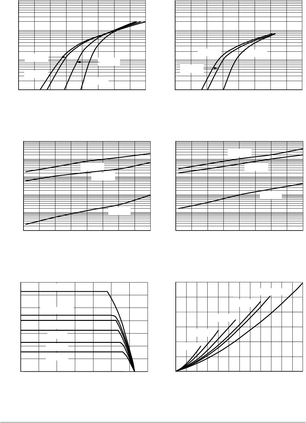
. . . employing the Schottky Barrier principle in a metaltosilicon
power rectifier. Features epitaxial construction with oxide passivation
and metal overlay contact. Ideally suited for low voltage, high
frequency switching power supplies; free wheeling diodes and
polarity protection diodes.
Features
Compact Package with JBend Leads Ideal for Automated Handling
Highly Stable Oxide Passivated Junction
Guardring for OverVoltage Protection
Low Forward Voltage Drop
ESD Ratings:
Human Body Model = 3B (> 16000 V)
Machine Model = C (> 400 V)
AECQ101 Qualified and PPAP Capable
NRVB Prefix for Automotive and Other Applications Requiring
Unique Site and Control Change Requirements
All Packages are PbFree*
Mechanical Characteristics
Case: Molded Epoxy
Epoxy Meets UL94, VO at 1/8
Weight: 95 mg (approximately)
Maximum Temperature of 260C / 10 Seconds for Soldering
Cathode Polarity Band
Available in 12 mm Tape, 2500 Units per 13 inch Reel, Add “T3”
Suffix to Part Number
Finish: All External Surfaces Corrosion Resistant and Terminal
Leads are Readily Solderable
Marking: BKJL
*For additional information on our PbFree strategy and soldering details, please
download the ON Semiconductor Soldering and Mounting Techniques
Reference Manual, SOLDERRM/D.
http://onsemi.com
Device Package Shipping
ORDERING INFORMATION
SMB
CASE 403A
SCHOTTKY BARRIER
RECTIFIER
2.0 AMPERES
40 VOLTS
MARKING DIAGRAM
MBRS2040LT3G SMB
(PbFree)
2,500 /
Tape & Reel
For information on tape and reel specifications,
including part orientation and tape sizes, please
refer to our Tape and Reel Packaging Specifications
Brochure, BRD8011/D.
NRVBS2040LT3G SMB
(PbFree)
2,500 /
Tape & Reel
BKJL = Specific Device Code
A = Assembly Location
Y = Year
WW = Work Week
G = PbFree Package
AYWW
BKJLG
G
(Note: Microdot may be in either location)
MBRS2040LT3G, NRVBS2040LT3G
http://onsemi.com
2
MAXIMUM RATINGS
Rating Symbol Value Unit
Peak Repetitive Reverse Voltage
Working Peak Reverse Voltage
DC Blocking Voltage
V
RRM
V
RWM
V
R
40 V
Average Rectified Forward Current
(At Rated V
R
, T
C
= 103C)
I
O
2.0
A
Peak Repetitive Forward Current
(At Rated V
R
, Square Wave, 20 kHz, T
C
= 104C)
I
FRM
4.0
A
NonRepetitive Peak Surge Current
(Surge Applied at Rated Load Conditions Halfwave, Single Phase, 60 Hz)
I
FSM
70
A
Storage Temperature T
stg
, T
C
55 to +150 C
Operating Junction Temperature T
J
55 to +125 C
Voltage Rate of Change
(Rated V
R
, T
J
= 25C)
dv/dt
10,000
V/ms
Stresses exceeding Maximum Ratings may damage the device. Maximum Ratings are stress ratings only. Functional operation above the
Recommended Operating Conditions is not implied. Extended exposure to stresses above the Recommended Operating Conditions may affect
device reliability.
THERMAL CHARACTERISTICS
Characteristic
Symbol Value Unit
Thermal Resistance — JunctiontoLead (Note 1)
Thermal Resistance — JunctiontoAmbient (Note 2)
R
JL
R
JA
22.5
78
C/W
1. Minimum pad size (0.108 X 0.085 inch) for each lead on FR4 board.
2. 1 inch square pad size (1 x 0.5 inch for each lead) on FR4 board.
ELECTRICAL CHARACTERISTICS
Characteristic
Symbol Value Unit
Maximum Instantaneous Forward Voltage (Note 3)
see Figure 2
(I
F
= 2.0 A)
(I
F
= 4.0 A)
V
F
T
J
= 25C T
J
= 125C
Volts
0.43
0.50
0.34
0.45
Maximum Instantaneous Reverse Current (Note 3)
see Figure 4
(V
R
= 40 V)
(V
R
= 20 V)
I
R
T
J
= 25C T
J
= 100C
mA
0.8
0.1
20
6.0
3. Pulse Test: Pulse Width 250 s, Duty Cycle 2.0%.
MBRS2040LT3G, NRVBS2040LT3G
http://onsemi.com
3
Figure 1. Typical Forward Voltage Figure 2. Maximum Forward Voltage
Figure 3. Typical Reverse Current Figure 4. Maximum Reverse Current
Figure 5. Current Derating Figure 6. Forward Power Dissipation
0
v
F
, INSTANTANEOUS FORWARD VOLTAGE (VOLTS)
100
10
1.0
V
F
, MAXIMUM INSTANTANEOUS FORWARD VOLTAGE (VOLTS)
0
1.0
0.1
400
V
R
, REVERSE VOLTAGE (VOLTS)
100E-3
10E-3
1.0E-3
100E-6
10E-6
1.0E-6
V
R
, REVERSE VOLTAGE (VOLTS)
20 600
T
L
, LEAD TEMPERATURE (C)
3.5
2.0
1.5
1.0
0.5
0
I
O
, AVERAGE FORWARD CURRENT (AMPS)
0.50
1.2
1.0
0.8
0.6
0.2
0
2.040
i
F
, INSTANTANEOUS FORWARD CURRENT (AMPS)
I
0.1
0.60.2 0.4 0.8 0.2 0.4 0.6 0.8
10
100
10 20 30
, AVERAGE FORWARD CURRENT (AMPS)I
O
80 120100
2.5
1.0 1.5 2.5 3.0
0.4
P
FO
, AVERAGE POWER DISSIPATION (WATTS)
I
F
, INSTANTANEOUS FORWARD CURRENT (AMPS)
, REVERSE CURRENT (AMPS)
R
400
V
R
, REVERSE VOLTAGE (VOLTS)
100E-3
10E-3
1.0E-3
100E-6
10E-6
1.0E-6
I
10 20 30
, MAXIMUM REVERSE CURRENT (AMPS)
R
140
3.0
T
J
= 125C
T
J
= 100C
T
J
= -40C
T
J
= 25C
T
J
= 125C
T
J
= 100C
T
J
= 25C
T
J
= 125C
T
J
= 100C
T
J
= 25C
T
J
= 125C
T
J
= 100C
T
J
= 25C
SQUARE WAVE
dc
I
pk
/I
o
= p
I
pk
/I
o
= 5
I
pk
/I
o
= 10
I
pk
/I
o
= 20
I
pk
/I
o
= 20
I
pk
/I
o
= 10
I
pk
/I
o
= 5
I
pk
/I
o
= p
SQUARE WAVE
dc
100

MBRS2040LT3G

Mfr. #:
Manufacturer:
ON Semiconductor
Description:
Schottky Diodes & Rectifiers 2A 40V Low Vf
Lifecycle:
New from this manufacturer.
Delivery:
DHL FedEx Ups TNT EMS
Payment:
T/T Paypal Visa MoneyGram Western Union

Products related to this Datasheet