© Semiconductor Components Industries, LLC, 1994
October, 2016 − Rev. 12
1 Publication Order Number:
BAS116LT1/D
BAS116L
Switching Diode
Features
• Low Leakage Current Applications
• Medium Speed Switching Times
• Available in 8 mm Tape and Reel
Use BAS116LT1G to order the 7 inch/3,000 unit reel
• S and NSV Prefix for Automotive and Other Applications Requiring
Unique Site and Control Change Requirements; AEC−Q101
Qualified and PPAP Capable
• These Devices are Pb−Free, Halogen Free/BFR Free and are RoHS
Compliant
MAXIMUM RATINGS
Rating Symbol Value Unit
Continuous Reverse Voltage V
R
75 Vdc
Peak Forward Current I
F
200 mAdc
Peak Forward Surge Current I
FM(surge)
500 mAdc
THERMAL CHARACTERISTICS
Characteristic Symbol Max Unit
Total Device Dissipation FR−5 Board (Note 1)
T
A
= 25°C
Derate above 25°C
P
D
225
1.8
mW
mW/°C
Thermal Resistance, Junction−to−Ambient
R
q
JA
556 °C/W
Total Device Dissipation
Alumina Substrate (Note 2) T
A
= 25°C
Derate above 25°C
P
D
300
2.4
mW
mW/°C
Thermal Resistance, Junction−to−Ambient
R
q
JA
417 °C/W
Junction and Storage Temperature T
J
, T
stg
−55 to
+150
°C
Stresses exceeding those listed in the Maximum Ratings table may damage
the device. If any of these limits are exceeded, device functionality should not
be assumed, damage may occur and reliability may be affected.
1. FR−5 = 1.0 0.75 0.062 in.
2. Alumina = 0.4 0.3 0.024 in. 99.5% alumina.
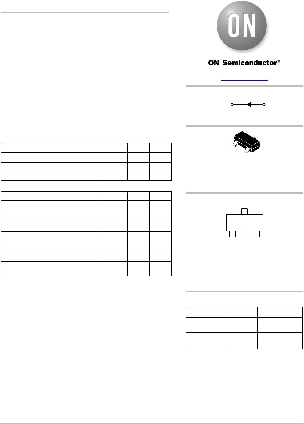
3
CATHODE
1
ANODE
Device Package Shipping
†
ORDERING INFORMATION
SOT−23 (TO−236)
CASE 318
STYLE 8
MARKING DIAGRAM
1
2
3
JV M G
G
BAS116LT1G
SBAS116LT1G
SOT−23
(Pb−Free)
3000 / Tape & Ree
JV = Specific Device Code
M = Date Code*
G = Pb−Free Package
(Note: Microdot may be in either location)
*Date Code orientation and/or overbar may
vary depending upon manufacturing location.
BAS116LT3G
NSVBAS116LT3G
SOT−23
(Pb−Free)
10000 / Tape &
Reel
†For information on tape and reel specifications,
including part orientation and tape sizes, please
refer to our Tape and Reel Packaging Specification
Brochure, BRD8011/D.
www.onsemi.com