LTC4231
16
4321fa
For more information www.linear.com/LTC4231
applicaTions inForMaTion
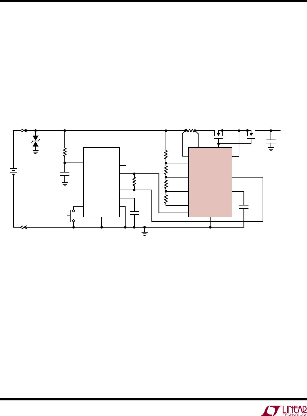
Supply Transient Protection
When the capacitances at the input and output are very
small, rapid changes in current during an output short-
circuit event can cause transients that exceed the 40V
absolute maximum ratings of IN, SENSE and SOURCE.
To minimize such spikes, use wider traces or heavier
trace plating to reduce the power trace inductance. Also,
bypass locally with a 10μF electrolytic and 0.1μF ceramic
if hot plug inrush current is not a concern. Alternatively,
clamp the input with a transient voltage suppressor (Z1
in Figure 5). A 10Ω, 0.1μF snubber damps the response
and reduces ringing (R
X
and C
X
in Figure 5).
Design Example
As a design example, take the following specifications for
the Figure 5 application circuit. The application is rated
for a V
IN
of 24V at 2A, C
L
= 100µF. UV rising = 23V, UV
falling = 22V, OV rising = 26V.
Sense resistor:
R
SENSE
=
SENSE(CB)(MIN)
=
47mV
= 23.5mΩ
Use R
SENSE
= 22.5mΩ for margin. Worst case analog
current limit:
I
LIMIT(MIN)
=
SENSE(ACL)(MIN)
22.5mΩ
=
65mV
22.5mΩ
= 2.89A
I
LIMIT(MAX)
=
∆V
SENSE(ACL)(MAX)
=
90mV
= 4A
Calculate the worst case time it takes to charge up C
L
in
analog current limit:
t
CHARGE(MAX)
=
L
IN
I
LIMIT(MIN)
=
2.89A
= 0.9ms
For inrush control using analog current limit, t
CHARGE(MAX)
must be less than the circuit breaker delay (t
CB
) for a
proper start-up.
The worst case power dissipation in MOSFET M1 occurs
during a severe overcurrent fault when the current is
controlled by analog current limit for the duration of t
CB
:
P
DISS
= V
IN
• I
LIMIT(MAX)
= 24V • 4A = 96W
The SOA (safe operating area) curve for the Si7164DP
MOSFET shows that it can withstand 180W for 10ms. So
choose a t
CB
that is less than 10ms but higher than 0.9ms
(t
CHARGE(MAX)
). In this case, use t
CB
= 2ms.
C
T
=
CB
=
= 0.082µF = 82nF
If a low inrush current (< ∆V
SENSE(CB)
) is preferred, refer to
the Figure 1 application circuit which uses a gate capaci-
tor C
G
to limit the inrush current. Choose I
INRUSH
= 0.5A
which is set using C
G
:
C
G
=
L
I
INRUSH
• 10µA =
0.5A
• 10µA = 20nF
The time to charge up C
L
with 0.5A is:
t
CHARGE
=
L
IN
I
=
0.5A
= 48ms
In this case t
CHARGE
can be longer than t
CB
with no start-
up issue.
The average power dissipation in the MOSFET M1 during
this start-up is:
P
DISS
=
IN
INRUSH
=
24V • 0.5A
= 6W
The SOA of the MOSFET M1 must be evaluated to ensure
that it can withstand 6W for 48ms. The SOA curve of the
Si7120ADN withstands 10W for 360ms, satisfying the
requirement.
The purpose of MOSFET M2 is to block the reverse path
from OUT (drain of M2) to IN when GATE pulls to GND so
that IN can go lower than OUT or even negative. Choose a
40V MOSFET to withstand a worse case reverse DC volt
-
age of
–24
V. The Si5410DU offers a good choice with a
maximum R
DS(ON)
of 18mΩ at V
GS
= 10V.