LTC4231
20
4321fa
For more information www.linear.com/LTC4231
Information furnished by Linear Technology Corporation is believed to be accurate and reliable.
However, no responsibility is assumed for its use. Linear Technology Corporation makes no representa-
tion that the interconnection of its circuits as described herein will not infringe on existing patent rights.
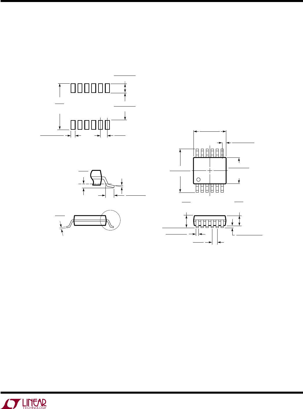
package DescripTion
UD Package
12-Lead Plastic QFN (3mm × 3mm)
(Reference LTC DWG # 05-08-1855 Rev Ø)
Please refer to http://www.linear.com/designtools/packaging/ for the most recent package drawings.
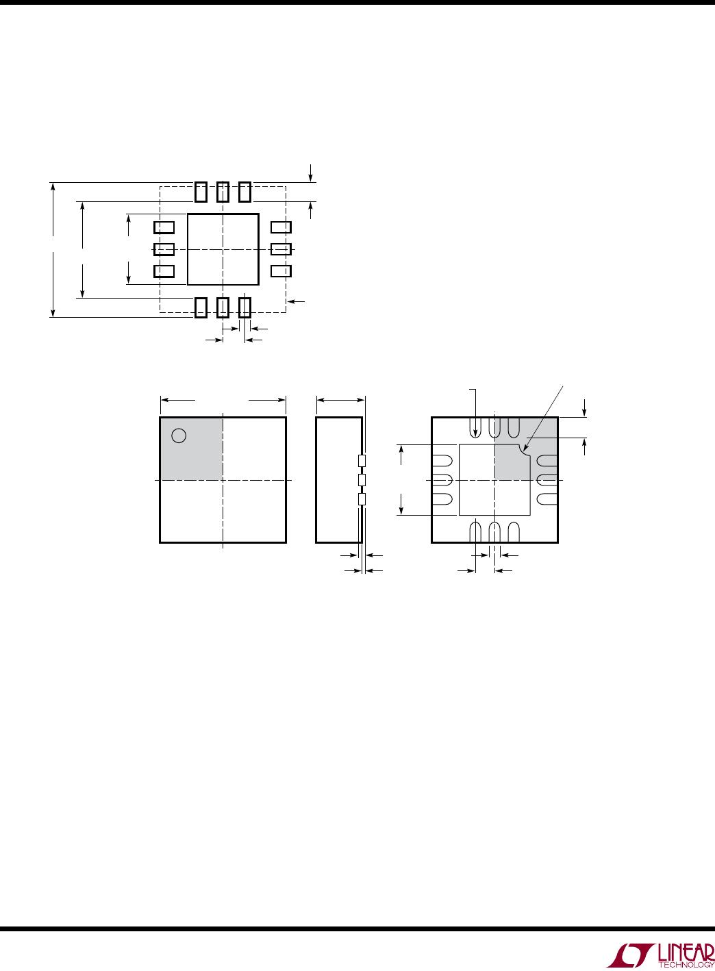
3.00 ± 0.10
(4 SIDES)
RECOMMENDED SOLDER PAD PITCH AND DIMENSIONS
1.65 ±0.05
(4 SIDES)
NOTE:
1. DRAWING CONFORMS TO JEDEC PACKAGE OUTLINE MO-220 VARIATION (WEED-1)
2. DRAWING NOT TO SCALE
3. ALL DIMENSIONS ARE IN MILLIMETERS
4. DIMENSIONS OF EXPOSED PAD ON BOTTOM OF PACKAGE DO NOT INCLUDE
MOLD FLASH. MOLD FLASH, IF PRESENT, SHALL NOT EXCEED 0.15mm ON ANY SIDE
5. EXPOSED PAD SHALL BE SOLDER PLATED
6. SHADED AREA IS ONLY A REFERENCE FOR PIN 1 LOCATION
ON THE TOP AND BOTTOM OF PACKAGE
PIN 1
TOP MARK
(NOTE 6)
0.40 ±0.10
BOTTOM VIEW—EXPOSED PAD
1.65 ±0.10
(4-SIDES)
0.75 ±0.05
R = 0.115
TYP
0.25 ±0.05
1
PIN 1 NOTCH R = 0.20 TYP
OR 0.25 × 45° CHAMFER
11 12
2
0.50 BSC
0.200 REF
2.10 ±0.05
3.50 ±0.05
0.70 ±0.05
0.00 – 0.05
(UD12) QFN 0709 REV Ø
0.25 ±0.05
0.50 BSC
PACKAGE OUTLINE
UD Package
12-Lead Plastic QFN (3mm × 3mm)
(Reference LTC DWG # 05-08-1855 Rev Ø)