Expand menu
Hello, Sign in
My Account
0
Cart
Home
Products
Sensors
Semiconductors
Passive Components
Connectors
Power
Electromechanical
Optoelectronics
Circuit Protection
Integrated Circuits - ICs
Main Products
Manufacturers
Blog
Services
About OMO
About Us
Contact Us
Check Stock
AT17F080-30JU
P1-P3
P4-P6
P7-P9
P10-P12
P13-P14
AT17F040/080 [DATASHEET]
Atmel-3039M-CNFG-AT17F040-080-Datasheet_012015
10
10.
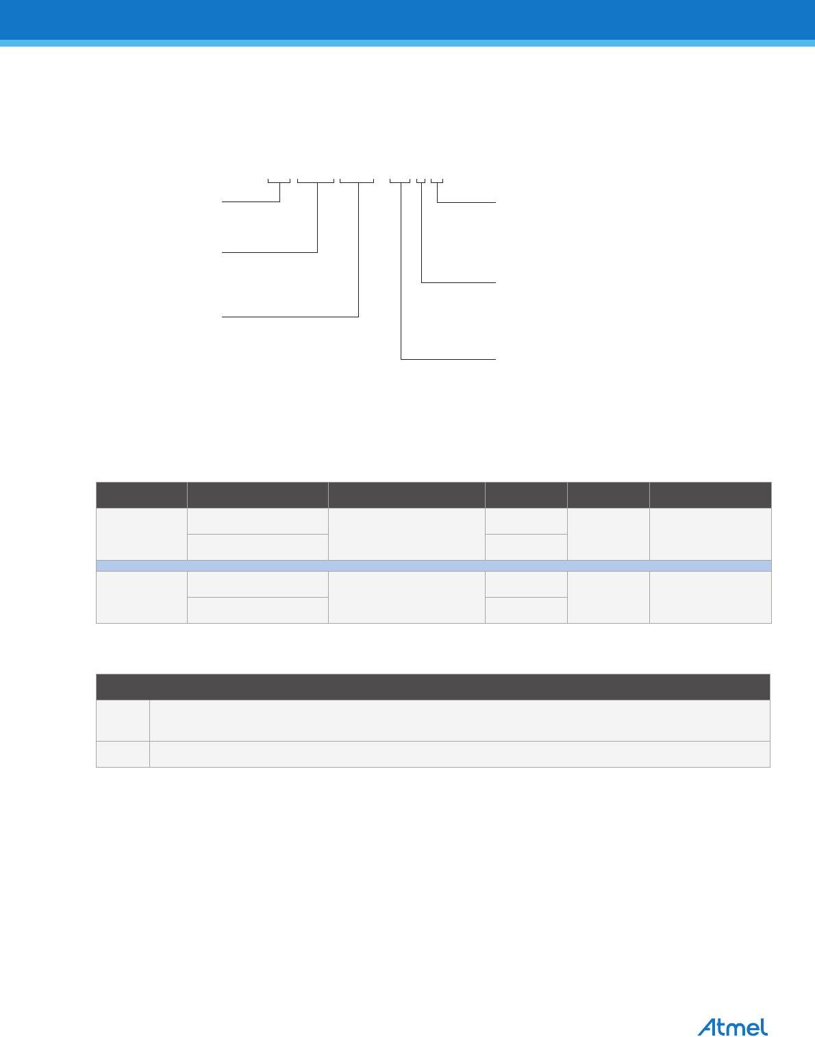
Ordering Information
10.1
Ordering Code Detail
10.2
Ordering Information
A
T17F040-30CU
Atmel Designator
Product Family
Device Density
Package Option
Product Variation
040 = 4 megabit
080 = 8 megabit
17F = FPGA Flash
Configuration Memory
Package Device Grade
C
= 8-pad LAP
J
= 20-lead PLCC
U
=
Green, Sn Lead Finish
Industrial Temperature Range
(-40°C to +85°C)
30 = Default Value
Memory Size
Atmel Ordering Code
Lead Finish
Package
Voltage
Operation Range
4-Mbit
AT17F040-30CU
Sn
(Lead-free/Halogen-free)
8CN4
3.3V
Industrial
(-40
C to 85
C)
AT17F040-30JU
20J
8-Mbit
AT17F080-30CU
Sn
(Lead-free/Halogen-free)
8CN4
3.3V
Industrial
(-40
C to 85
C)
AT17F080-30JU
20J
Package Type
8CN4
8-pad, 6mm x 6mm x 1.04mm, Leadless Array Package (LAP)
Pin-compatible with 8-lead SOIC/VOIC Packages
20J
20-lead, Plastic J-leaded Chip Carrier (PLCC)
11
AT17F040/080 [DATASHEET]
Atmel-3039M-CNFG-AT17F040-080-Datasheet_012015
11.
Packaging Information
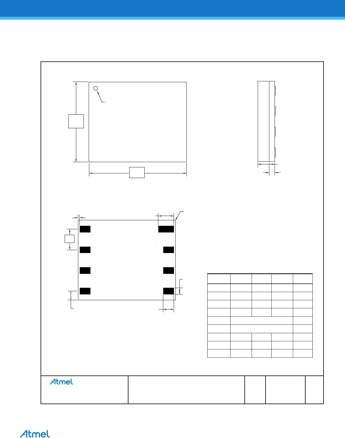
11.1
8CN4 — 8-pad LAP
DRA
WING NO
.
REV
.
TITLE
GPC
8CN4
E
12/22/14
8CN4, 8-pad 6x6x1.04mm Body
, 1.27mm pitch
Leadless
Array Package (LAP)
DMH
Package Drawing Contact:
packagedrawings@atmel.com
COMMON DIMENSIONS
(Unit of Measure = mm)
SYMBOL
MIN
TYP
MAX
NOTE
A
0.94
1.04
1.14
A1
0.30
0.34
0.38
D
5.89
5.99
6.09
E
5.89
5.99
6.09
e
1.27 BSC
e1
1.10 REF
L
0.95
1.00
1.05
1
L1
1.25
1.30
1.35
1
b
0.45
0.50
0.55
1
Pin1 Corner
Marked Pin1 Indentifier
0.10 mm
TYP
4
3
2
1
5
6
7
8
T
op View
L
b
e
L1
e1
Side View
A1
A
Bottom View
E
D
Note:
1. Metal Pad Dimensions.
2.
All exposed metal area shall have the following finished platings.
Ni: 0.0005 to 0.015 mm
Au: 0.0005 to 0.001 mm
AT17F040/080 [DATASHEET]
Atmel-3039M-CNFG-AT17F040-080-Datasheet_012015
12
11.2
20J — 20-lead PLCC
TITLE
DRA
WING NO
.
REV
.
Notes:
1.
This package conforms to JEDEC reference MS-018, Variation AA
2.
Dimensions D1 and E1 do not include mold protrusion.
Allowable protrusion is .010"(0.254mm) per side. Dimension D1
and E1 include mold mismatch and are measured at the extreme
material condition at the upper or lower parting line.
3.
Lead coplanarity is 0.004" (0.102mm) maximum
A
4.191
–
4.572
A1
2.286
–
3.048
A2
0.508
–
–
D
9.779
–
10.033
D1
8.890
–
9.042
Note
2
E
9.779
–
10.033
E1
8.890
–
9.042
Note
2
D2/E2 7.366
–
8.382
B
0.660
–
0.813
B1
0.330
–
0.533
e
1.270
TYP
COMMON DIMENSIONS
(Unit of Measure = mm)
SYMBOL
MIN
NOM
MAX
NOTE
1.14(0.045) X 45°
PIN NO
. 1
IDENTIFIER
1.14(0.045) X 45°
0.51(0.020)MAX
0.318(0.0125)
0.191(0.0075)
A2
45° MAX (3X)
A
A1
B1
D2/E2
B
e
E1
E
D1
D
20J
, 20-lead, Plastic J-leaded Chip Carrier (PLCC)
B
20J
10/04/01
Package Drawing Contact:
packagedrawings@atmel.com
P1-P3
P4-P6
P7-P9
P10-P12
P13-P14
AT17F080-30JU
Mfr. #:
Buy AT17F080-30JU
Manufacturer:
Microchip Technology / Atmel
Description:
FPGA - Configuration Memory FPGA SERIAL CONFIG 30MHZ IND TEMP GREEN
Lifecycle:
New from this manufacturer.
Delivery:
DHL
FedEx
Ups
TNT
EMS
Payment:
T/T
Paypal
Visa
MoneyGram
Western
Union
Products related to this Datasheet
AT17F080-30CU
AT17F040-30CU
AT17F040-30JU
AT17F080-30JU