3
COMMERCIAL AND INDUSTRIAL TEMPERATURE RANGES
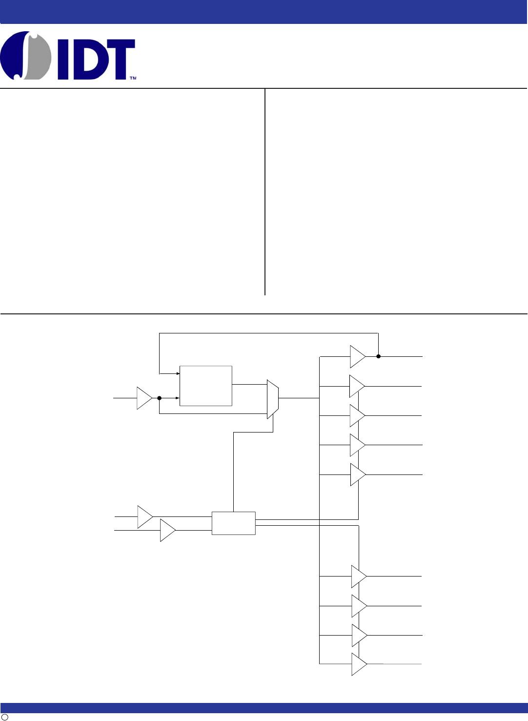
IDT2309
3.3V ZERO DELAY CLOCK BUFFER
DC ELECTRICAL CHARACTERISTICS - COMMERCIAL
Symbol Parameter Conditions Min. Max. Unit
VIL Input LOW Voltage Level — 0.8 V
VIH Input HIGH Voltage Level 2 — V
IIL Input LOW Current VIN = 0V — 50 µA
IIH Input HIGH Current VIN = VDD — 100 µA
VOL Output LOW Voltage Standard Drive IOL = 8mA — 0.4 V
High Drive IOL = 12mA (-1H)
VOH Output HIGH Voltage Standard Drive IOH = -8mA 2.4 — V
High Drive IOH = -12mA (-1H)
IDD_PD Power Down Current REF = 0MHz (S2 = S1 = H) — 12 µA
IDD Supply Current Unloaded Outputs at 66.66MHz, SEL inputs at VDD or GND — 32 mA
SWITCHING CHARACTERISTICS (2309-1) - COMMERCIAL
(1,2)
Symbol Parameter Conditions Min. Typ. Max. Unit
t1 Output Frequency 10pF Load 10 — 133 MHz
30pF Load 10 — 100
Duty Cycle = t2 ÷ t1 Measured at 1.4V, FOUT = 66.66MHz 40 50 60 %
t3 Rise Time Measured between 0.8V and 2V — — 2.5 ns
t4 Fall Time Measured between 0.8V and 2V — — 2.5 ns
t5 Output to Output Skew All outputs equally loaded — — 250 ps
t6A Delay, REF Rising Edge to CLKOUT Rising Edge
(2)
Measured at VDD/2 — 0 ±350 ps
t6B Delay, REF Rising Edge to CLKOUT Rising Edge
(2)
Measured at VDD/2 in PLL bypass mode (IDT2309 only) 1 5 8.7 ns
t7 Device-to-Device Skew Measured at VDD/2 on the CLKOUT pins of devices — 0 700 ps
tJ Cycle-to-Cycle Jitter Measured at 66.66MHz, loaded outputs — — 200 ps
t
LOCK PLL Lock Time Stable power supply, valid clock presented on REF pin — — 1 ms
NOTES:
1. REF Input has a threshold voltage of VDD/2.
2. All parameters specified with loaded outputs.
Symbol Parameter Min. Max. Unit
VDD Supply Voltage 3 3.6 V
TA Operating Temperature (Ambient Temperature) 0 70 °C
CL Load Capacitance < 100MHz — 30 pF
Load Capacitance 100MHz - 133MHz — 10
CIN Input Capacitance — 7 pF
OPERATING CONDITIONS - COMMERCIAL
FUNCTION TABLE
(1)
S2 S1 CLKA CLKB CLKOUT
(2)
Output Source PLL Shut Down
L L Tri-State Tri-State Driven PLL N
L H Driven Tri-State Driven PLL N
H L Driven Driven Driven REF Y
H H Driven Driven Driven PLL N
NOTES:
1. H = HIGH Voltage Level.
L = LOW Voltage Level
2. This output is driven and has an internal feedback for the PLL. The load on this ouput can be adjusted to change the skew between the REF and the output.