1/9
■ VERY LOW POWER CONSUMPTION :
10µA/op
■ OUTPUT VOLTAGE CAN SWING TO
GROUND
■ EXCELLENT PHASE MARGIN ON
CAPACITIVE LOADS
■ STABLE AND LOW OFFSET VOLTAGE
■ THREE INPUT OFFSET VOLTAGE
SELECTIONS
DESCRIPTION
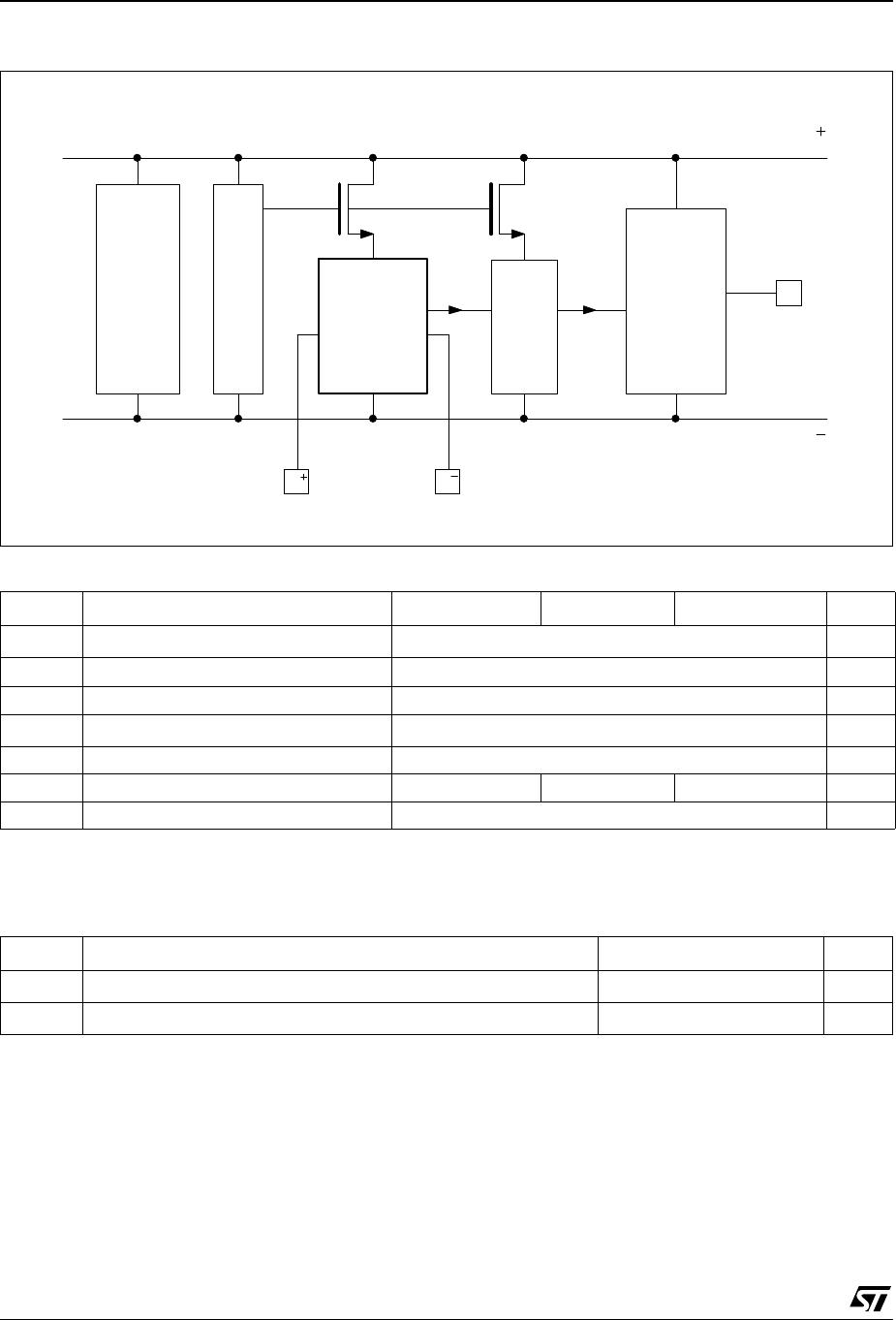
These devices are low cost, low power dual oper-
ational amplifiers designed to operate with single
or dual supplies. These operational amplifiers use
the ST silicon gate CMOS process allowing an ex-
cellent consumption-speed ratio. These series are
ideally suited for low consumption applications.
Three power consumptions are available allowing
to have always the best consumption-speed ratio:
❑ I
CC
= 10µA/amp.: TS27L2 (very low power)
❑ I
CC
= 150µA/amp.: TS27M2 (low power)
❑ I
CC
= 1mA/amp.: TS272 (standard)
These CMOS amplifiers offer very high input im-
pedance and extremely low input currents. The
major advantage versus JFET devices is the very
low input currents drift with temperature (see fig-
ure 2).
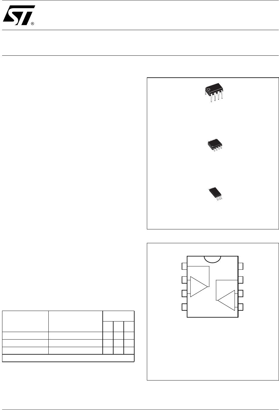
ORDER CODE
N = Dual in Line Package (DIP)
D = Small Outline Package (SO) - also available in Tape & Reel (DT)
P = Thin Shrink Small Outline Package (TSSOP) - only available
in Tape & Reel (PT)
PIN CONNECTIONS (top view)
Part Number Temperature Range
Package
NDP
TS27L2C/AC/BC 0°C, +70°C
•••
TS27L2I/AI/BI -40°C, +125°C
•••
TS27L2M/AM/BM -55°C, +125°C
•••
Example : TS27L2ACN
N
DIP8
(Plastic Package)
D
SO8
(Plastic Micropackage)
P
TSSOP8
(Thin Shrink Small Outline Package)
1
2
3
45
6
7
8
CC
+
-
-
+
-
+
CC
1 - Output 1
2 - Inverting Input 1
3 - Non-inverting Input 1
4 - V
5 - Non-inverting Input 2
6 - Inverting Input 2
7 - Output 2
8 - V
TS27L2C,I,M
PRECISION VERY LOW POWER
CMOS DUAL OPERATIONAL AMPLIFIERS
November 2001