ADuM240D/ADuM240E/ADuM241D/ADuM241E/ADuM242D/ADuM242E Data Sheet
Rev. A | Page 22 of 26
APPLICATIONS INFORMATION
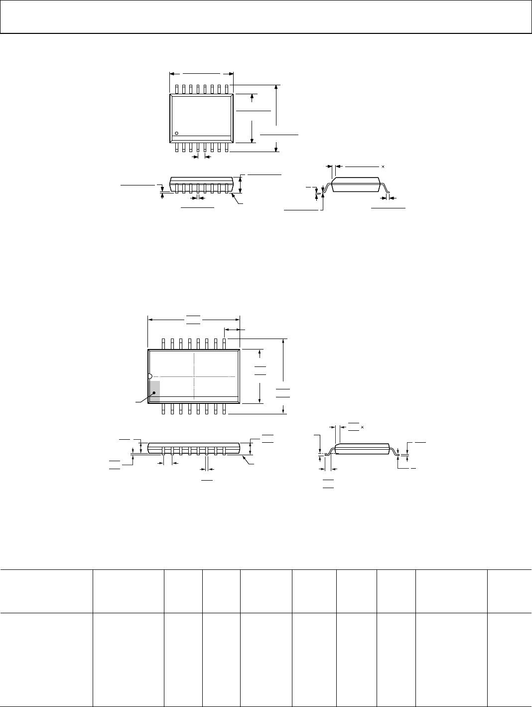
PCB LAYOUT
The ADuM240D/ADuM240E/ADuM241D/ADuM241E/
ADuM242D/ADuM242E digital isolators require no external
interface circuitry for the logic interfaces. Power supply bypassing
is strongly recommended at the input and output supply pins
(see Figure 21). Bypass capacitors are most conveniently connected
between Pin 1 and Pin 2 for V
DD1
and between Pin 15 and Pin 16
for V
DD2
. The recommended bypass capacitor value is between
0.01 μF and 0.1 μF. The total lead length between both ends of
the capacitor and the input power supply pin must not exceed
10 mm. Bypassing between Pin 1 and Pin 8 and between Pin 9
and Pin 16 must also be considered, unless the ground pair on
each package side is connected close to the package.
Figure 21. Recommended Printed Circuit Board Layout
In applications involving high common-mode transients, ensure
that board coupling across the isolation barrier is minimized.
Furthermore, design the board layout such that any coupling
that does occur equally affects all pins on a given component
side. Failure to ensure this can cause voltage differentials between
pins exceeding the Absolute Maximum Ratings of the device,
thereby leading to latch-up or permanent damage.
See the AN-1109 Application Note for board layout guidelines.
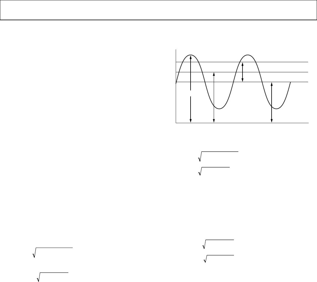
PROPAGATION DELAY RELATED PARAMETERS
Propagation delay is a parameter that describes the time
required for a logic signal to propagate through a component. The
propagation delay to a Logic 0 output may differ from the
propagation delay to a Logic 1 output.
Figure 22. Propagation Delay Parameters
Pulse width distortion is the maximum difference between these
two propagation delay values and is an indication of how
accurately the timing of the input signal is preserved.
Channel matching is the maximum amount the propagation
delay differs between channels within a single ADuM240D/
ADuM240E/ADuM241D/ADuM241E/ADuM242D/ADuM242E
component.
Propagation delay skew is the maximum amount the propagation
delay differs between multiple ADuM240D/ADuM240E/
ADuM241D/ADuM241E/ADuM242D/ADuM242E components
operating under the same conditions
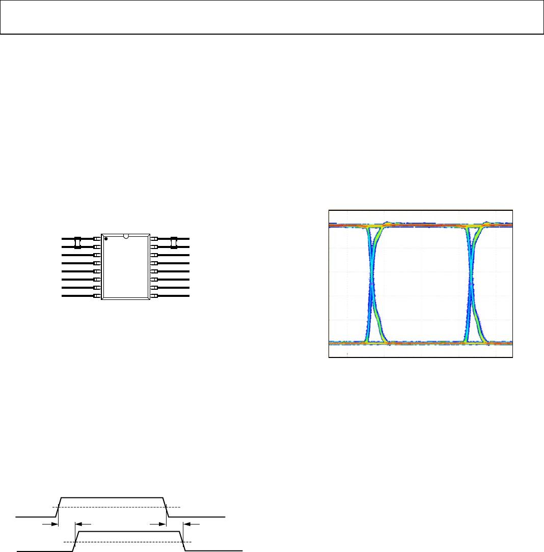
JITTER MEASUREMENT
Figure 23 shows the eye diagram for the ADuM240D/ADuM240E/
ADuM241D/ADuM241E/ADuM242D/ADuM242E. The
measurement was taken using an Agilent 81110A pulse pattern
generator at 150 Mbps with pseudorandom bit sequences (PRBS)
2(n − 1), n = 14, for 5 V supplies. Jitter was measured with the
Tektronix Model 5104B oscilloscope, 1 GHz, 10 GSPS with the
DPOJET jitter and eye diagram analysis tools. The result shows a
typical measurement on the ADuM240D/ADuM240E/
ADuM241D/ADuM241E/ADuM242D/ADuM242E with
490 ps p-p jitter.
Figure 23. ADuM240D/ADuM240E/ADuM241D/ADuM241E/ADuM242D/
ADuM242E Eye Diagram
INSULATION LIFETIME
All insulation structures eventually break down when subjected
to voltage stress over a sufficiently long period. The rate of
insulation degradation is dependent on the characteristics of the
voltage waveform applied across the insulation as well as on the
materials and material interfaces.
The two types of insulation degradation of primary interest are
breakdown along surfaces exposed to the air and insulation
wear out. Surface breakdown is the phenomenon of surface
tracking, and the primary determinant of surface creepage
requirements in system level standards. Insulation wear out is the
phenomenon where charge injection or displacement currents
inside the insulation material cause long-term insulation
degradation.
Surface Tracking
Surface tracking is addressed in electrical safety standards by
setting a minimum surface creepage based on the working voltage,
the environmental conditions, and the properties of the insulation
material. Safety agencies perform characterization testing on the
surface insulation of components that allows the components to be
categorized in different material groups. Lower material group
ratings are more resistant to surface tracking and, therefore, can
provide adequate lifetime with smaller creepage. The minimum
creepage for a given working voltage and material group is in each
V
DD1
GND
1
V
IA
V
IB
V
IC
/V
OC
V
ID
/V
OD
DISABLE
1
/V
E1
/NIC
GND
1
V
DD2
GND
2
V
OA
V
OB
V
IC
/V
OC
V
ID
/V
OD
DISABLE
2
/V
E2
/NIC
GND
2
13576-010
INPUT (V
Ix
)
OUTPUT (V
Ox
)
t
PLH
t
PHL
50%
50%
13576-011
105
0
1
2
3
4
VOL
AGE (V)
5
0
TIME (ns)
–5–10
13576-012