IR2151
2
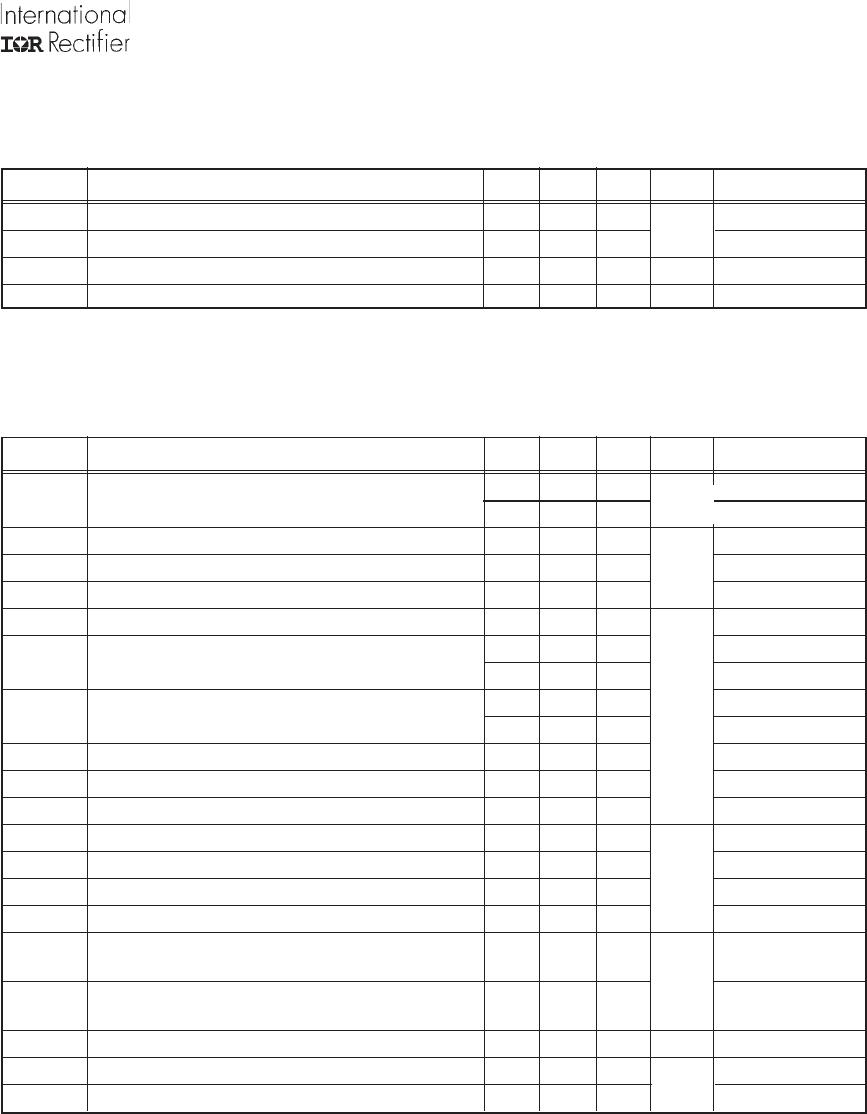
Symbol Definition Min. Max. Units
V
B
High side floating supply voltage -0.3 625
V
S
High side floating supply offset voltage V
B
- 25 V
B
+ 0.3
V
HO
High side floating output voltage V
S
- 0.3 V
B
+ 0.3
V
LO
Low side output voltage -0.3 V
CC
+ 0.3
V
RT
R
T
voltage -0.3 V
CC
+ 0.3
V
CT
C
T
voltage -0.3 V
CC
+ 0.3
I
CC
Supply current (note 1) — 25
I
RT
R
T
output current -5 5
dV
s
/dt Allowable offset supply voltage transient — 50 V/ns
P
D
Package power dissipation @ T
A
≤ +25°C (8 lead DIP) — 1.0
(8 lead SOIC) — 0.625
R
θJA Thermal resistance, junction to ambient (8 lead DIP) — 125
(8 lead SOIC) — 200
T
J
Junction temperature — 150
T
S
Storage temperature -55 150 °C
T
L
Lead temperature (soldering, 10 seconds) — 300
Absolute Maximum Ratings
Absolute maximum ratings indicate sustained limits beyond which damage to the device may occur. All voltage param-
eters are absolute voltages referenced to COM. The thermal resistance and power dissipation ratings are measured
under board mounted and still air conditions.
V
°C/W
W
mA
structure between the chip V
CC
and COM which has a nominal breakdown voltage of 15.6V. Therefore, the IC
supply voltage is normally derived by forcing current into the supply lead (typically by means of a high value
resistor connected between the chip V
CC
and the rectified line voltage and a local decoupling capacitor from
V
CC
to COM) and allowing the internal zener clamp circuit to determine the nominal supply voltage. There-
fore, this circuit should not be driven by a DC, low impedance power source of greater than V
CLAMP
.
Note 1: Because of the IR2151’s application specificity toward off-line supply systems, this IC contains a zener clamp
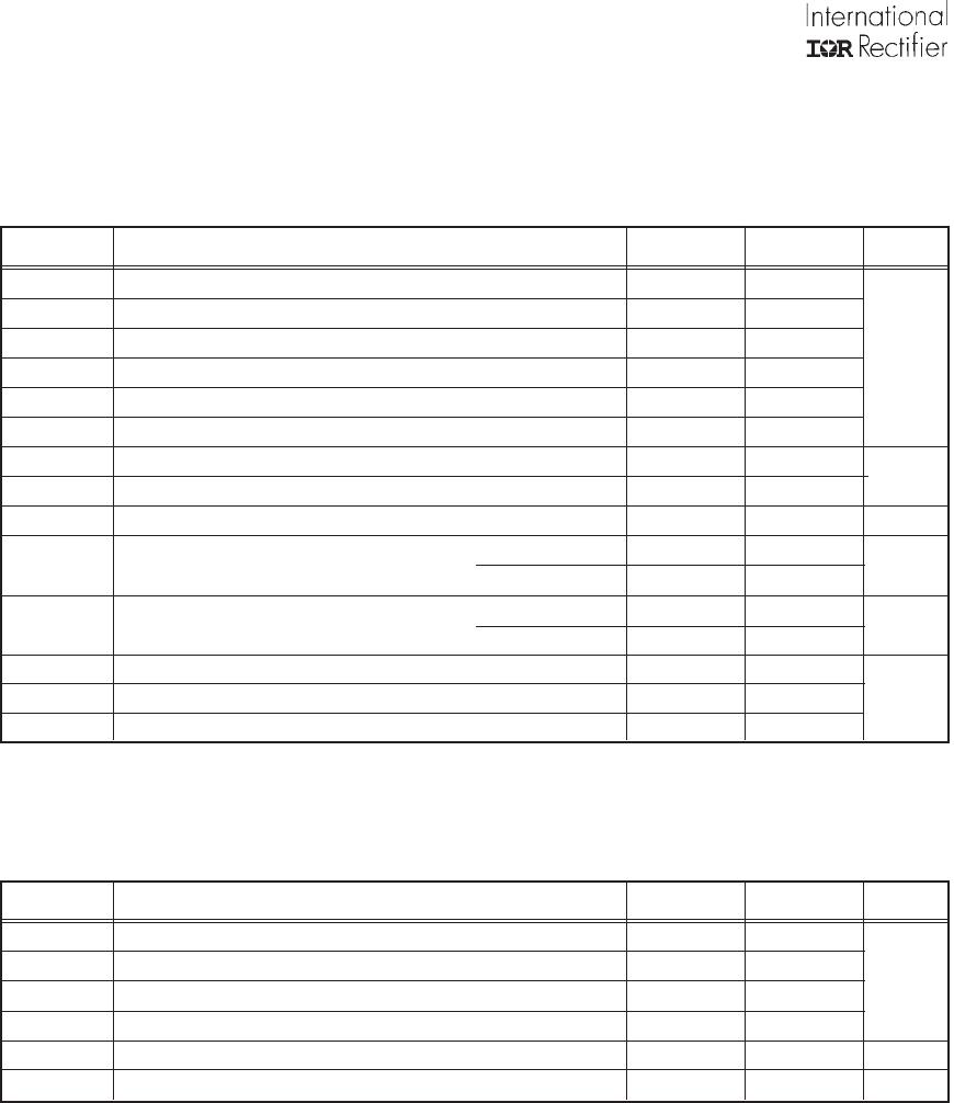
Symbol Definition Min. Max. Units
V
B
High side sloating supply absolute voltage V
S
+ 10 V
S
+ 20
V
S
High side floating supply offset voltage — 600
V
HO
High side floating output voltage V
S
V
B
V
LO
Low side output voltage 0 V
CC
I
CC
Supply current (note 1) — 5 mA
T
A
Ambient temperature -40 125 °C
Recommended Operating Conditions
The input/output logic timing diagram is shown in figure 1. For proper operation the device should be used within the
recommended conditions. The V
S
offset rating is tested with all supplies biased at 15V differential.
V