© Semiconductor Components Industries, LLC, 2014
June, 2014 − Rev. 3
1 Publication Order Number:
NVTFS5116PL/D
NVTFS5116PL
Power MOSFET
−60 V, −14 A, 52 mW, Single P−Channel
Features
• Small Footprint (3.3 x 3.3 mm) for Compact Design
• Low R
DS(on)
to Minimize Conduction Losses
• Low Capacitance to Minimize Driver Losses
• NVTFS5116PLWF − Wettable Flanks Product
• AEC−Q101 Qualified and PPAP Capable
• These Devices are Pb−Free and are RoHS Compliant
MAXIMUM RATINGS (T
J
= 25°C unless otherwise noted)
Parameter
Symbol Value Unit
Drain−to−Source Voltage V
DSS
−60 V
Gate−to−Source Voltage V
GS
±20 V
Continuous Drain Cur
rent R
Y
J−mb
(Notes 1,
2, 3, 4)
Steady
State
T
mb
= 25°C
I
D
−14
A
T
mb
= 100°C −10
Power Dissipation
R
Y
J−mb
(Notes 1, 2, 3
T
mb
= 25°C
P
D
21
W
T
mb
= 100°C 10
Continuous Drain Cur
rent R
q
JA
(Notes 1 &
3, 4)
Steady
State
T
A
= 25°C
I
D
−6
A
T
A
= 100°C −4
Power Dissipation
R
q
JA
(Notes 1, 3)
T
A
= 25°C
P
D
3.2
W
T
A
= 100°C 1.6
Pulsed Drain Current
T
A
= 25°C, t
p
= 10 ms
I
DM
−126 A
Operating Junction and Storage Temperature T
J
, T
stg
−55 to
+175
°C
Source Current (Body Diode) I
S
−17 A
Single Pulse Drain−to−Source Avalanche
Energy (T
J
= 25°C, V
DD
= 50 V, V
GS
= 10 V,
I
L(pk)
= 30 A, L = 0.1 mH, R
G
= 25 W)
E
AS
45 mJ
Lead Temperature for Soldering Purposes
(1/8″ from case for 10 s)
T
L
260 °C
Stresses exceeding those listed in the Maximum Ratings table may damage the
device. If any of these limits are exceeded, device functionality should not be
assumed, damage may occur and reliability may be affected.
THERMAL RESISTANCE MAXIMUM RATINGS (Note 1)
Parameter
Symbol Value Unit
Junction−to−Mounting Board (top) − Steady
State (Note 2 and 3)
R
Y
J−mb
7.2
°C/W
Junction−to−Ambient − Steady State (Note 3)
R
q
JA
47
1. The entire application environment impacts the thermal resistance values shown,
they are not constants and are only valid for the particular conditions noted.
2. Psi (Y) is used as required per JESD51−12 for packages in which
substantially less than 100% of the heat flows to single case surface.
3. Surface−mounted on FR4 board using a 650 mm
2
, 2 oz. Cu pad.
4. Continuous DC current rating. Maximum current for pulses as long as 1
second is higher but is dependent on pulse duration and duty cycle.
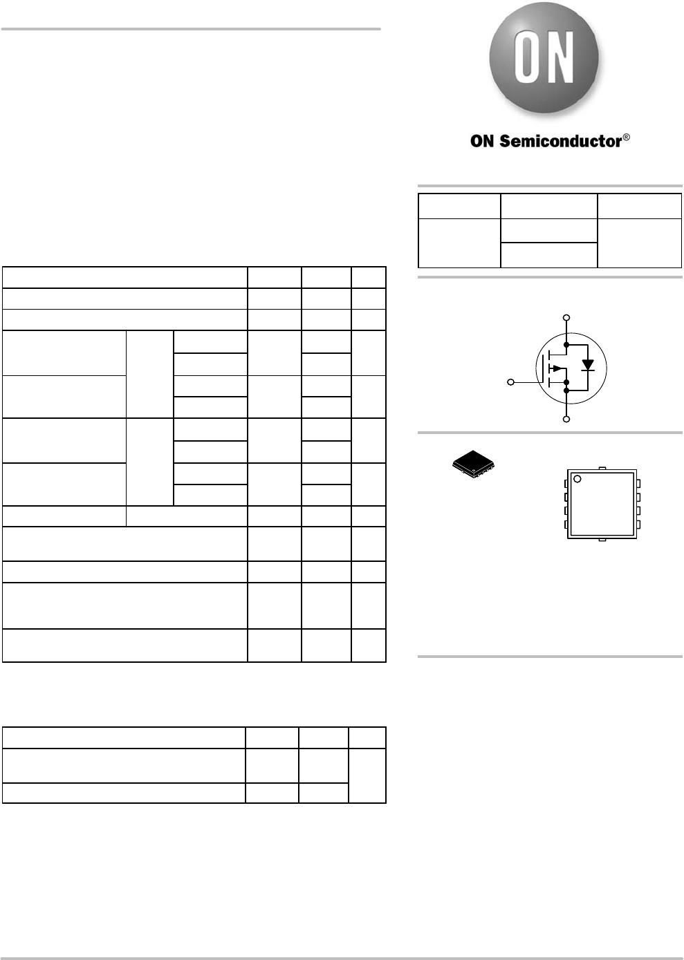
http://onsemi.com
V
(BR)DSS
R
DS(on)
MAX I
D
MAX
−60 V
52 mW @ −10 V
−14 A
P−Channel MOSFET
D (5−8)
S (1,2,3)
G (4)
WDFN8
(m8FL)
CASE 511AB
MARKING DIAGRAM
72 mW @ −4.5 V
(Note: Microdot may be in either location)
1
XXXX = Specific Device Code
A = Assembly Location
Y = Year
WW = Work Week
G = Pb−Free Package
1
XXXX
AYWWG
G
D
D
D
D
S
S
S
G
See detailed ordering, marking and shipping information in the
package dimensions section on page 5 of this data sheet.
ORDERING INFORMATION

