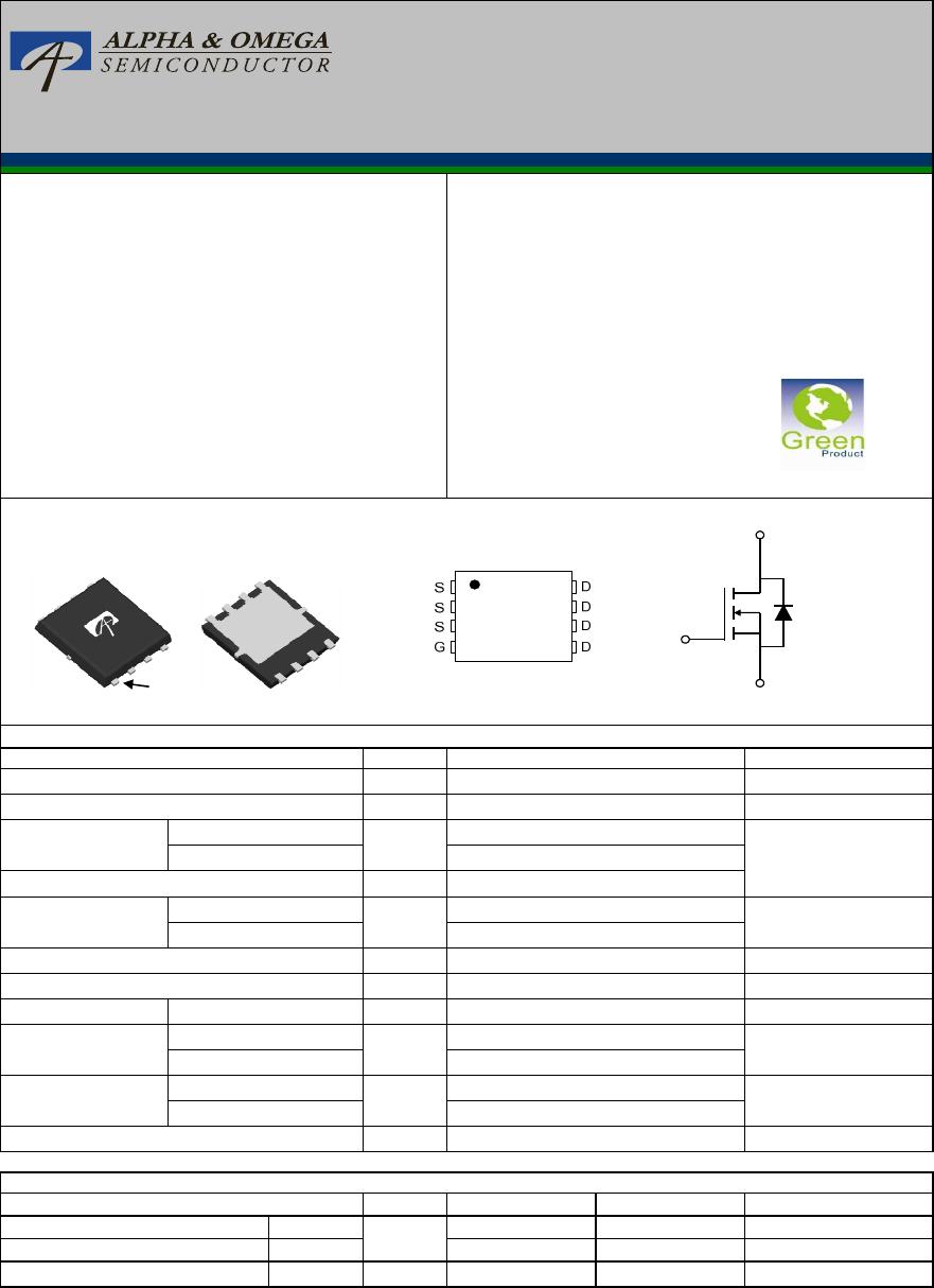
AON6500
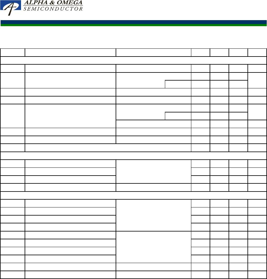
Symbol Min Typ Max Units
BV
DSS
30 V
V
DS
=30V, V
GS
=0V 1
T
J
=55°C 5
I
GSS
100 nA
V
GS(th)
Gate Threshold Voltage
1 1.4 2 V
0.75 0.95
T
J
=125°C 1.1 1.4
1 1.3 mΩ
g
FS
100 S
V
SD
0.7 1 V
I
S
100 A
C
iss
7036 pF
C
oss
2778 pF
C
rss
353 pF
R
g
0.5 1.1 1.7 Ω
Q
g
(10V) 107 145 nC
Q
g
(4.5V) 49.7 68 nC
Q
gs
11.7 nC
Q
gd
21.4 nC
t
D(on)
12.3 ns
t
r
12.8 ns
I
DSS
Diode Forward Voltage
DYNAMIC PARAMETERS
V
GS
=4.5V, I
D
=20A
V
GS
=10V, I
D
=20A
Gate-Body leakage current
V
DS
=0V, V
GS
= ±20V
I
S
=1A,V
GS
=0V
Maximum Body-Diode Continuous Current
µA
Drain-Source Breakdown Voltage
Electrical Characteristics (T
J
=25°C unless otherwise noted)
STATIC PARAMETERS
Parameter Conditions
I
D
=250µA, V
GS
=0V
Gate Source Charge
V
GS
=10V, V
DS
=15V, I
D
=20A
Turn-On Rise Time
Zero Gate Voltage Drain Current
mΩ
Reverse Transfer Capacitance
V
GS
=0V, V
DS
=15V, f=1MHz
V
DS
=V
GS,
I
D
=250µA
Output Capacitance
Gate Drain Charge
Total Gate Charge
V
GS
=10V, V
DS
=15V, R
L
=0.75Ω,
R
DS(ON)
Static Drain-Source On-Resistance
Gate resistance
Forward Transconductance
SWITCHING PARAMETERS
Turn-On DelayTime
V
GS
=0V, V
DS
=0V, f=1MHz
Total Gate Charge
V
DS
=5V, I
D
=20A
Input Capacitance
D(off)
t
f
28.8 ns
t
rr
31 ns
Q
rr
106
nC
THIS PRODUCT HAS BEEN DESIGNED AND QUALIFIED FOR THE CONSUMER MARKET. APPLICATIONS OR USES AS CRITICAL
COMPONENTS IN LIFE SUPPORT DEVICES OR SYSTEMS ARE NOT AUTHORIZED. AOS DOES NOT ASSUME ANY LIABILITY ARISING
OUT OF SUCH APPLICATIONS OR USES OF ITS PRODUCTS. AOS RESERVES THE RIGHT TO IMPROVE PRODUCT DESIGN,
FUNCTIONS AND RELIABILITY WITHOUT NOTICE.
Turn-Off Fall Time
Body Diode Reverse Recovery Charge
Body Diode Reverse Recovery Time
I
F
=20A, dI/dt=500A/µs
I
F
=20A, dI/dt=500A/µs
GEN
A. The value of R
θJA
is measured with the device mounted on 1in
2
FR-4 board with 2oz. Copper, in a still air environment with T
A
=25°C. The
Power dissipation P
DSM
is based on R
θJA
and the maximum allowed junction temperature of 150°C. The value in any given application depends
on the user's specific board design.
B. The power dissipation P
D
is based on T
J(MAX)
=150°C, using junction-to-case thermal resistance, and is more useful in setting the upper
dissipation limit for cases where additional heatsinking is used.
C. Single pulse width limited by junction temperature T
J(MAX)
=150°C.
D. The R
θJA
is the sum of the thermal impedance from junction to case R
θJC
and case to ambient.
E. The static characteristics in Figures 1 to 6 are obtained using <300µs pulses, duty cycle 0.5% max.
F. These curves are based on the junction-to-case thermal impedance which is measured with the device mounted to a large heatsink, assuming
a maximum junction temperature of T
J(MAX)
=150°C. The SOA curve provides a single pulse rating.
G. The maximum current rating is package limited.
H. These tests are performed with the device mounted on 1 in
2
FR-4 board with 2oz. Copper, in a still air environment with T
A
=25°C.
Rev 0: Jan 2012 www.aosmd.com Page 2 of 6