3
LTC2901
2901fb
The ● denotes the specifications which apply over the full operating
temperature range, otherwise specifications are at T
A
= 25°C. V
CC
= 5V, unless otherwise noted. (Notes 3, 4)
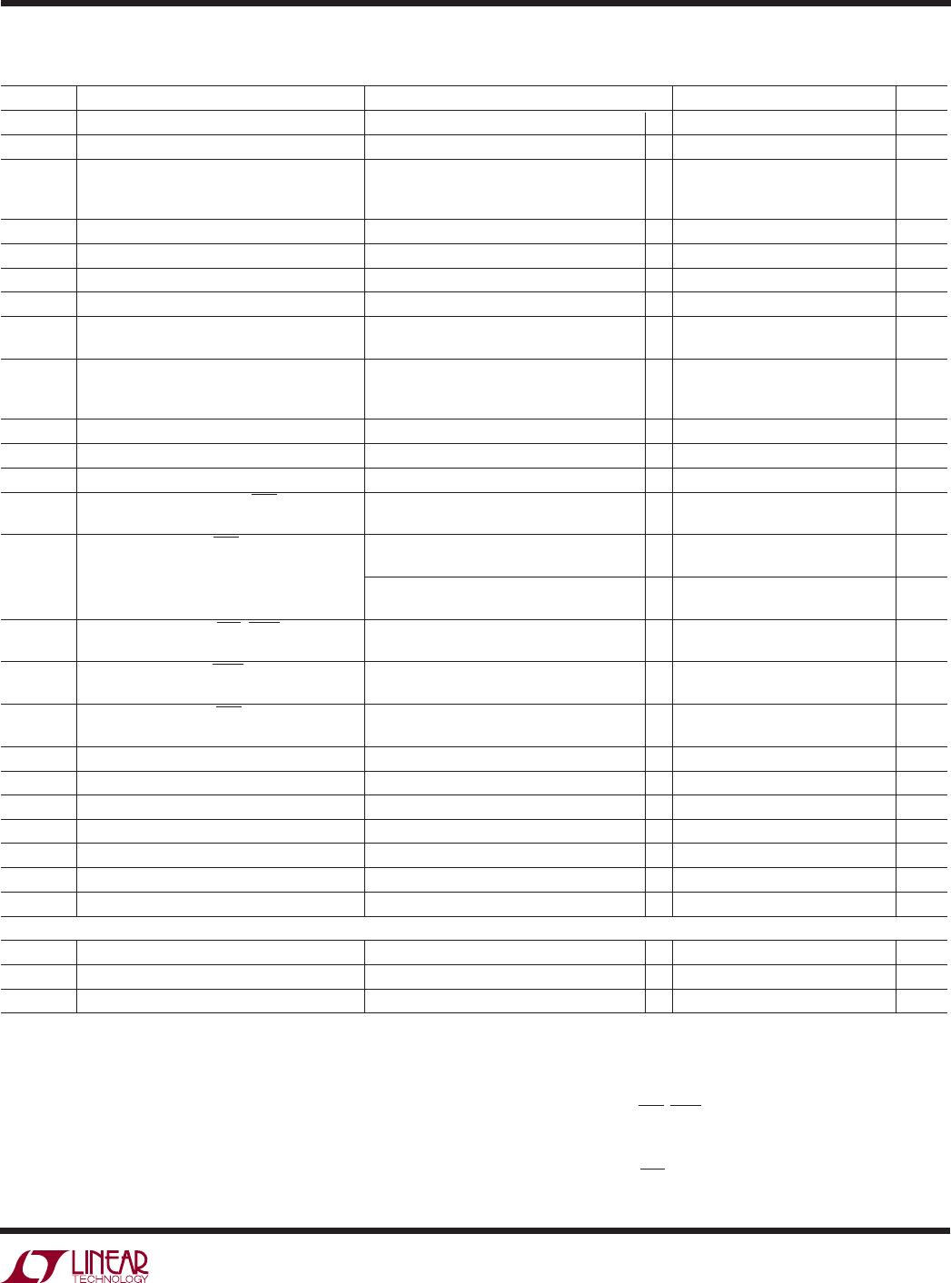
ELECTRICAL CHARACTERISTICS
Note 1: Stresses beyond those listed under Absolute Maximum Ratings may
cause permanent damage to the device. Exposure to any Absolute Maximum
Rating condition for extended periods may affect device reliability and
lifetime.
Note 2: All currents into pins are positive, all voltages are referenced to GND
unless otherwise noted.
Note 3: The greater of V1, V2 is the internal supply voltage (V
CC
).
Note 4: 10% thresholds apply to the LTC2901-3/LTC2901-4 only when the
TOL pin is set to a logic high.
Note 5: Under static no-fault conditions, V1 will necessarily supply quiescent
current. If at any time V2 is larger than V1, V2 must be capable of supplying
the quiescent current, programming (transient) current and reference load
current.
Note 6: The output pins RST, WDO and COMPX have internal pull-ups to V2
of typically 6μA. However, external pull-up resistors may be used when faster
rise times are required or for V
OH
voltages greater than V2.
Note 7: The push-pull RST output pin on the LTC2901-2/LTC2901-4 is
actively
pulled up to V2.
SYMBOL PARAMETER CONDITIONS MIN TYP MAX UNITS
V
CCMINP
Minimum Required for Programming V
CC
Rising ● 2.42 V
V
CCMINC
Minimum Required for Comparators V
CC
Falling ● 2.32 V
V
REF
Reference Voltage V
CC
≥ 2.3V, I
VREF
= ±1mA, C
REF
≤ 1000pF
T0L Low
● 1.192 1.210 1.228 V
T0L High
● 1.128 1.146 1.163 V
V
PG
Programming Voltage Range V
CC
≥ V
CCMINP
● 0V
REF
V
I
VPG
V
PG
Input Current V
PG
= V
REF
● ±20 nA
I
V1
V1 Input Current V1 = 5V, I
VREF
= 12μA, (Note 5) ● 43 75 μA
I
V2
V2 Input Current V2 = 3.3V ● 0.8 2 μA
I
V3
V3 Input Current V3 = 2.5V ● 0.52 1.2 μA
V3 = 0.55V (ADJ Mode)
● –15 15 nA
I
V4
V4 Input Current V4 = 1.8V ● 0.34 0.8 μA
V4 = 0.55V (ADJ Mode) ● –15 15 nA
V4 = –0.05V (–ADJ Mode)
● –15 15 nA
I
CRT(UP)
CRT Pull-Up Current V
CRT
= 0V ● –1.4 –2 –2.6 μA
I
CRT(DN)
CRT Pull-Down Current V
CRT
= 1.3V ● 10 20 30 μA
t
RST
Reset Time-Out Period C
RT
= 1500pF ● 579 ms
t
UV
V
X
Undervoltage Detect to RST or COMPX V
X
Less Than Reset Threshold V
RTX
150 μs
by More Than 1%
V
OL
Output Voltage Low RST, COMPX I
SINK
= 2.5mA; V1 = 3V, V2 = 3V; ● 0.15 0.4 V
V3, V4 = 0V; V
PG
= 0V
I
SINK
= 100μA; V2 = 1V; V1, V3, V4 = 0V ● 0.05 0.3 V
I
SINK
= 100μA; V1 = 1V; V2, V3, V4 = 0V ● 0.05 0.3 V
V
OH
Output Voltage High RST, WDO, COMPX I
SOURCE
= 1μA ● V2 – 1 V
(Note 6)
V
OL
Output Voltage Low WDO I
SINK
= 2.5mA; V1 = 5V, V2 = 3.3V; ● 0.15 0.4 V
V3, V4 = 1V; V
PG
= 0V
V
OH
Output Voltage High RST I
SOURCE
= 200μA ● 0.8 • V2 V
(LTC2901-2/LTC2901-4) (Note 7)
I
CWT(UP)
CWT Pull-Up Current V
CWT
= 0V ● –1.4 –2 –2.6 μA
I
CWT(DN)
CWT Pull-Down Current V
CWT
= 1.3V ● 10 20 30 μA
t
WD
Watchdog Time-Out Period C
WT
= 1500pF ● 20 30 40 ms
V
IH
WDI Input Threshold High V
CC
= 3.3V to 5.5V ● 1.6 V
V
IL
WDI Input Threshold Low V
CC
= 3.3V to 5.5V ● 0.4 V
t
WP
WDI Input Pulse Width V
CC
= 3.3V ● 150 ns
I
WDI
WDI Pull-Up Current V
WDI
= 0V –10 μA
Digital Input T0L
V
IL
T0L Low Level Input Voltage V
CC
= 3.3V to 5.5V ● 0.3V
CC
V
V
IH
T0L High Level Input Voltage V
CC
= 3.3V to 5.5V ● 0.7V
CC
V
I
INTOL
T0L Input Current TOL = V
CC
● ±0.1 ±1 μA