11
LTC2901
2901fb
APPLICATIO S I FOR ATIO
WUUU
Power-Up
The greater of V1, V2 is the internal supply voltage (V
CC
).
On power-up, V
CC
will power the drive circuits for the RST
and the COMPX pins. This ensures that the RST and COMPX
outputs will be low as soon as V1 or V2 reaches 1V. The
RST and COMPX outputs will remain low until the part is
programmed. After programming, if any one of the V
X
inputs
is below its programmed threshold, RST will be a logic low.
Once all the V
X
inputs rise above their thresholds, an inter-
nal timer is started and RST is released after the pro-
grammed delay time. If V
CC
< (V3 – 1) and V
CC
< 2.4V, the
V3 input impedance will be low (1kΩ typ).
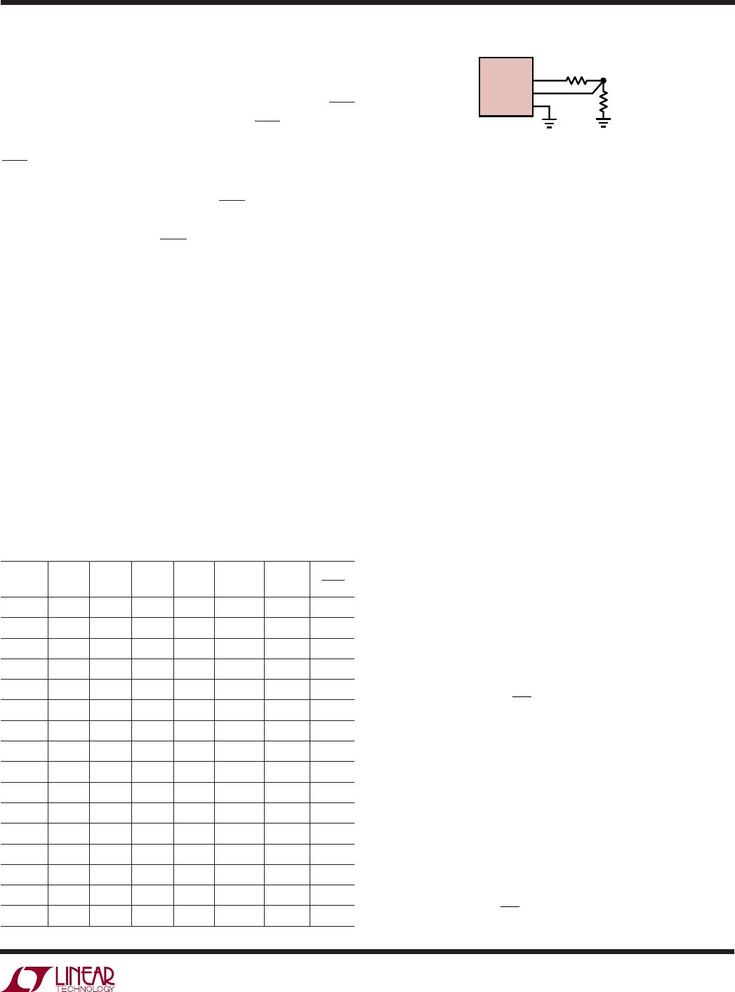
Monitor Programming
The LTC2901 input voltage combination is selected by
placing the recommended resistive divider from V
REF
to
GND and connecting the tap point to V
PG
, as shown in
Figure 4. Table 1 offers recommended 1% resistor values
for the various modes. The last column in Table 1 specifies
optimum V
PG
/V
REF
ratios (±0.01) to be used when pro-
gramming with a ratiometric DAC.
During power-up, once V1 or V2 reaches 2.4V max, the
monitor enters a programming period of approximately
150μs during which the voltage on the V
PG
pin is sampled
and the monitor is configured to the desired input combi-
nation. Do not add capacitance to the V
PG
pin. Immediately
after programming, the comparators are enabled and
supply monitoring will begin.
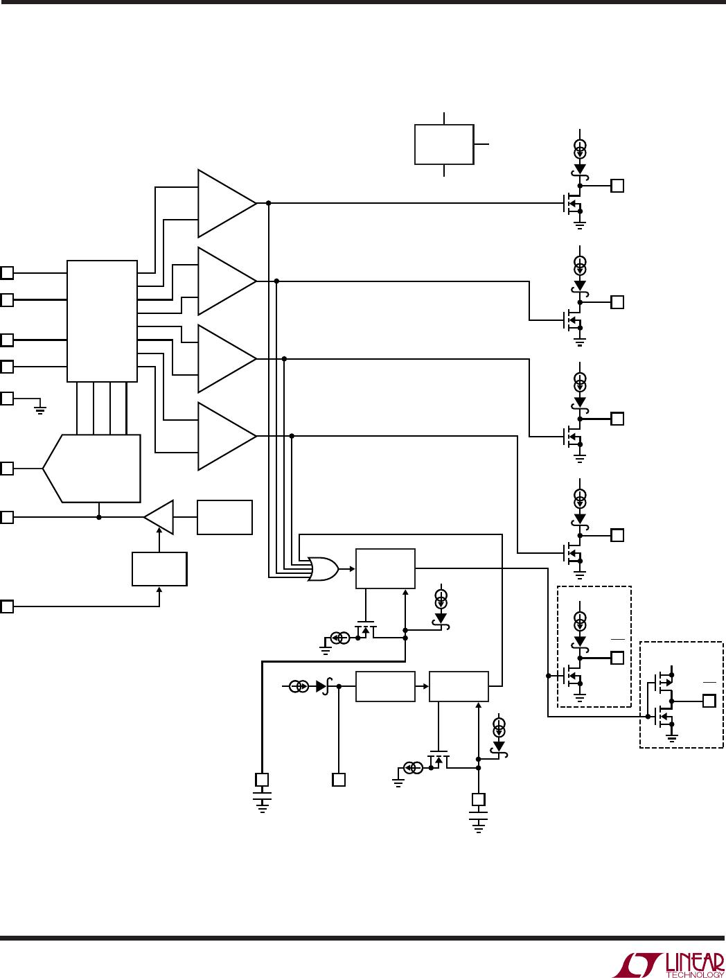
Supply Monitoring
The LTC2901 is a low power, high accuracy program-
mable quad supply monitoring circuit with four nondelayed
monitor outputs, a common reset output and a watchdog
timer. Watchdog and reset timing are both adjustable
using external capacitors. Single pin programming selects
1 of 16 input voltage monitor combinations. All four
voltage inputs must be above predetermined thresholds
for the reset not to be invoked. The LTC2901 will assert the
reset and comparator outputs during power-up, power-
down and brownout conditions on any one of the voltage
inputs.
The inverting inputs on the V3 and/or V4 comparators are
set to 0.5V when the positive adjustable modes are selected
(Figure 5). The tap point on an external resistive divider,
connected between the positive voltage being sensed and
ground, is connected to the high impedance noninverting
inputs (V3, V4). The trip voltage is calculated from:
VV
R
R
TRIP
=+
⎛
⎝
⎜
⎞
⎠
⎟
05 1
3
4
.
In the negative adjustable mode, the noninverting input on
the V4 comparator is connected to ground (Figure 6). The
tap point on an external resistive divider, connected be-
tween the negative voltage being sensed and the V
REF
pin,
is connected to the high impedance inverting input (V4).
V
REF
provides the necessary level shift required to operate
at ground. The trip voltage is calculated from:
VV
R
R
V V No al
TRIP REF REF
=
⎛
⎝
⎜
⎞
⎠
⎟
=– ; . min
3
4
1 210
Figure 4. Monitor Programming
12
11
10
R1
1%
R2
1%
2901 F04
V
REF
V
PG
GND
LTC2901
Table 1. Voltage Threshold Programming
V
PG
MODE V1 (V) V2 (V) V3 (V) V4 (V) R1 (kΩ) R2 (kΩ)V
REF
0 5.0 3.3 ADJ ADJ Open Short 0.000
1 5.0 3.3 ADJ –ADJ 93.1 9.53 0.094
2 3.3 2.5 ADJ ADJ 86.6 16.2 0.156
3 3.3 2.5 ADJ –ADJ 78.7 22.1 0.219
4 3.3 2.5 1.5 ADJ 71.5 28.0 0.281
5 5.0 3.3 2.5 ADJ 66.5 34.8 0.344
6 5.0 3.3 2.5 1.8 59.0 40.2 0.406
7 5.0 3.3 2.5 1.5 53.6 47.5 0.469
8 5.0 3.0 2.5 ADJ 47.5 53.6 0.531
9 5.0 3.0 ADJ ADJ 40.2 59.0 0.594
10 3.3 2.5 1.8 1.5 34.8 66.5 0.656
11 3.3 2.5 1.8 ADJ 28.0 71.5 0.719
12 3.3 2.5 1.8 –ADJ 22.1 78.7 0.781
13 5.0 3.3 1.8 –ADJ 16.2 86.6 0.844
14 5.0 3.3 1.8 ADJ 9.53 93.1 0.906
15 5.0 3.0 1.8 ADJ Short Open 1.000