8
LTC2901
2901fb
UU
U
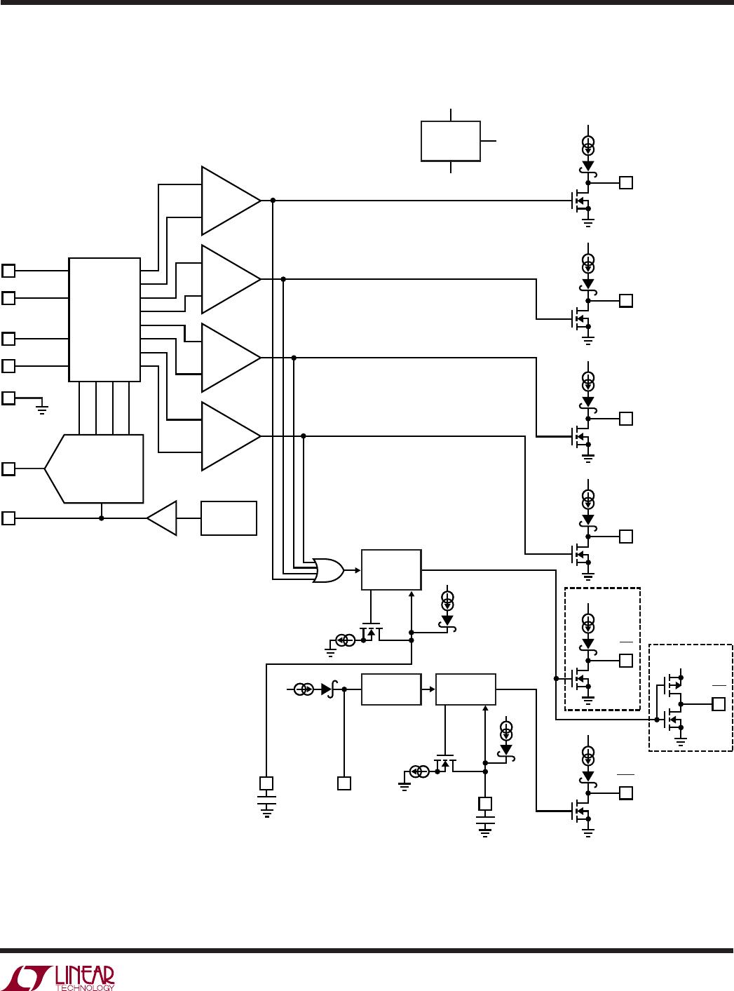
PI FU CTIO S
COMP3 (Pin 1): Comparator Output 3. Nondelayed, active
high logic output with weak pull-up to V2. Pulls high when
V3 is above reset threshold. May be pulled greater than V2
using external pull-up.
COMP1 (Pin 2): Comparator Output 1. Nondelayed, active
high logic output with weak pull-up to V2. Pulls high when
V1 is above reset threshold. May be pulled greater than V2
using external pull-up.
V3 (Pin 3): Voltage Input 3. Select from 2.5V, 1.8V, 1.5V
or ADJ. See Table 1 for details.
V1 (Pin 4): Voltage Input 1. Select from 5V or 3.3V. See
Table 1 for details. The greater of (V1, V2) is also V
CC
for
the device. Bypass this pin to ground with a 0.1μF (or
greater) capacitor.
CRT (Pin 5): Reset Delay Time Programming Pin. Attach
an external capacitor (C
RT
) to GND to set a reset delay time
of 4.6ms/nF. Leaving the pin open generates a minimum
delay of approximately 50μs. A 47nF capacitor will gener-
ate a 216ms reset delay time.
RST (Pin 6): Reset Logic Output. Active low with weak
pull-up to V2 (LTC2901-1/LTC2901-3) or active pull-up to
V2 (LTC2901-2/LTC2901-4). Pulls low when any voltage
input is below the reset threshold and held low for the
programmed delay time after all voltage inputs are above
threshold. May be pulled above V2 using an external pull-
up (LTC2901-1/LTC2901-3 only).
WDO (Pin 7): LTC2901-1/LTC2901-2 Watchdog Output.
Active low logic output with weak pull-up to V2. May be
pulled greater than V2 using external pull-up. The watch-
dog output pulls low if the watchdog timer is allowed to
time out and remains low until set high by the next WDI
transistion or anytime RST is low. The watchdog timer is
enabled when RST is high.
T0L (Pin 7): LTC2901-3/LTC2901-4 Digital Input for Sup-
ply Tolerance Selection (5% or 10%). A logic low selects
5% thresholds; a logic high selects 10% thresholds.
WDI (Pin 8): Watchdog Input. A logic input whose rising
or falling edge must occur on this pin (while RST is high)
within the selected watchdog time-out period, prohibiting
a high-to-low transition on the WDO pin (LTC2901-1/
LTC2901-2). The watchdog time-out period is set by the
value of the capacitor that is attached to the CWT pin.
A rising or falling edge on the WDI pin clears the voltage
on the C
WT
capacitor, preventing WDO from going low.
When disabling the watchdog function, tie CWT to GND.
For the LTC2901-3/LTC2901-4, a watchdog time-out due
to a missed WDI edge issues an RST pulse on the RST pin
(the WDO function is merged into the RST function).
CWT (Pin 9): Watchdog Time-Out Programming Pin.
Attach a capacitor (C
WT
) between CWT and GND to set a
watchdog time-out period of 20ms/nF. Leaving the pin
open generates a minimum time-out of approximately
200μs. A 47nF capacitor will generate a 940ms watchdog
time-out period.
GND (Pin 10): Ground.
V
PG
(Pin 11): Voltage Threshold Combination Select In-
put. Connect to an external 1% resistive divider between
V
REF
and GND to select 1 of 16 combinations of preset and/
or ±adjustable voltage thresholds (see Table 1). Do not
add capacitance on the V
PG
pin.
V
REF
(Pin 12): Buffered Reference Voltage. A 1.210V
nominal reference used for programming voltage (V
PG
)
and for the offset of negative adjustable applications. The
buffered reference can source and sink up to 1mA. The
reference can drive a bypass capacitor of up to 1000pF
without oscillation.
V4 (Pin 13): Voltage Input 4. Select from 1.8V, 1.5V, ADJ
or –ADJ. See Table 1 for details.
V2 (Pin 14): Voltage Input 2. Select from 3.3V, 3V or 2.5V.
See Table 1 for details. The greater of (V1, V2) is also V
CC
for device. Bypass this pin to ground with a 0.1μF (or
greater) capacitor. All logic outputs (COMP1, COMP2,
COMP3, COMP4, RST, WDO) are weakly pulled up to V2
(LTC2901-1/LTC2901-3). RST is actively pulled up to V2
in the LTC2901-2/LTC2901-4.
COMP4 (Pin 15): Comparator Output 4. Nondelayed,
active high logic output with weak pull-up to V2. Pulls high
when V4 is above reset threshold. May be pulled greater
than V2 using external pull-up.
COMP2 (Pin 16): Comparator Output 2. Nondelayed,
active high logic output with weak pull-up to V2. Pulls high
when V2 is above reset threshold. May be pulled greater
than V2 using external pull-up.