Si7439DP
www.vishay.com
Vishay Siliconix
S18-0353-Rev. F, 26-Mar-18
1
Document Number: 73106
For technical questions, contact: pmostechsupport@vishay.com
THIS DOCUMENT IS SUBJECT TO CHANGE WITHOUT NOTICE. THE PRODUCTS DESCRIBED HEREIN AND THIS DOCUMENT
ARE SUBJECT TO SPECIFIC DISCLAIMERS, SET FORTH AT www.vishay.com/doc?91000
P-Channel 150 V (D-S) MOSFET
FEATURES
• TrenchFET
®
power MOSFETs
• Ultra low on-resistance critical for application
• Low thermal resistance PowerPAK
®
package
with low 1.07 mm profile
• 100 % R
g
and avalanche tested
• Material categorization: for definitions of
compliance please see www.vishay.com/doc?99912
APPLICATIONS
• Active clamp in intermediate
DC/DC power supplies
Notes
a. Surface mounted on 1" x 1" FR4 board
b. See solder profile (www.vishay.com/doc?73257). The PowerP
AK SO-8 is a leadless package. The end of the lead terminal is exposed
copper (not plated) as a result of the singulation process in manufacturing. A solder fillet at the exposed copper tip cannot be guaranteed
and is not required to ensure adequate bottom side solder interconnection
c. Rework conditions: manual soldering with a soldering iron is not recommended for leadless components
PRODUCT SUMMARY
V
DS
(V) -150
R
DS(on)
max. () at V
GS
= -10 V 0.090
R
DS(on)
max. () at V
GS
= -6 V 0.095
Q
g
typ. (nC) 88,
I
D
(A) -5.2
Configuration Single
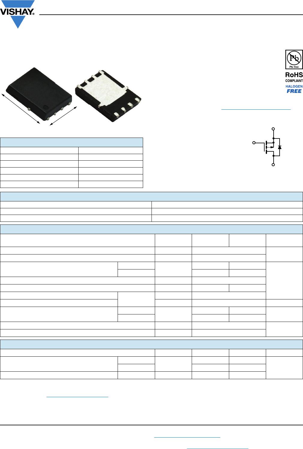
PowerPAK
®
SO-8 Single
Top View
1
6.15 mm
5.15 mm
Bottom View
4
G
3
S
2
S
1
S
D
8
D
6
D
7
D
5
Available
S
G
D
P-Channel MOSFE
ORDERING INFORMATION
Package PowerPAK SO-8
Lead (Pb)-free Si7439DP-T1-E3
Lead (Pb)-free and halogen-free Si7439DP-T1-GE3
ABSOLUTE MAXIMUM RATINGS (T
A
= 25 °C, unless otherwise noted)
PARAMETER SYMBOL 10 s
STEADY
STATE
UNIT
Drain-source voltage V
DS
-150
V
Gate-source voltage V
GS
± 20
Continuous drain current (T
J
= 150 °C)
a
T
A
= 25 °C
I
D
-5.2 -3
A
T
A
= 70 °C -4.1 -2.4
Pulsed drain current I
DM
-50
Continuous source current (diode conduction)
a
I
S
-4.2 -1.6
Single pulse avalanche current
L = 0.1 mH
I
AS
-40
Single pulse avalanche energy E
AS
80 mJ
Maximum power dissipation
a
T
A
= 25 °C
P
D
5.4 1.9
W
T
A
= 70 °C 3.4 1.2
Operating junction and storage temperature range T
J
, T
stg
-55 to 150
°C
Soldering recommendations (peak temperature)
b, c
260
THERMAL RESISTANCE RATINGS
PARAMETER SYMBOL TYPICAL MAXIMUM UNIT
Maximum junction-to-ambient
a
t 10 s
R
thJA
18 23
°C/WSteady state 50 65
Maximum junction-to-case (drain) Steady state R
thJC
11.5

