LT3032 Series
5
3032ff
For more information www.linear.com/LT3032
ELECTRICAL CHARACTERISTICS
The l denotes the specifications which apply over the full operating
temperature range, otherwise specifications are at T
A
= 25°C.
Note 1: Stresses beyond those listed under Absolute Maximum Ratings
may cause permanent damage to the device. Exposure to any Absolute
Maximum Rating condition for extended periods may affect device
reliability and lifetime.
Note 2: The LT3032 is tested and specified under pulse load conditions
such that T
J
≅ T
A
. The LT3032E is 100% tested at T
A
= 25°C. Performance
of the LT3032E over the full –40°C to 125°C operating junction
temperature range is assured by design, characterization, and correlation
with statistical process controls. The LT3032I regulators are guaranteed
over the full –40°C to 125°C operating junction temperature range.
Note 3: Parasitic diodes exist internally between the INN pin and the OUTN,
ADJN, and SHDNN pins. These pins cannot be pulled more than 0.5V
below the INN pin during fault conditions, and must remain at a voltage
more positive than the INN pin during operation.
Note 4: Operating conditions are limited by maximum junction
temperature. Specifications do not apply for all possible combinations of
input voltages and output currents. When operating at maximum input
voltages,
the output current ranges must be limited. When operating at
maximum output currents, the input voltage ranges must be limited.
Note 5:
The LT3032 is tested and specified for these conditions with the
ADJP pin tied to the OUTP pin and the ADJN pin tied to the OUTN pin.
Note 6: To satisfy requirements for minimum input voltage, the LT3032 is
tested and specified for these conditions with an external resistor divider
(two 250k resistors) from OUTP/OUTN to the corresponding ADJP/ADJN
pin to give an output voltage of ±2.44V. The external resistor divider adds
a 5µA DC load on the output. The LT3032-12/LT3032-15 have higher
internal resistor divider current, resulting in higher GND pin current at
light/no load.
Note 7: Dropout voltage is the minimum input-to-output voltage
differential needed to maintain regulation at a specified output current. In
dropout, output voltage equals:
V
INP/INN
– V
DROPOUT
For lower output voltages, dropout voltage is limited by the minimum
input voltage specification under some output voltage/load conditions;
see curves for Minimum INN Voltage and Minimum INP Voltage in Typical
Performance Characteristics. LT C is unable to guarantee Maximum
Dropout Voltage specifications at 50mA and 150mA
due to production
test limitations with Kelvin-Sensing the package pins. Please consult the
T
ypical Performance Characteristics for curves of Dropout Voltage as a
function of Output Load Current and Temperature.
Note 8: GND pin current is tested with V
INP
= V
OUTP(NOMINAL)
or V
INN
=
V
OUTN(NOMINAL)
and a current source load. This means the device is tested
while operating in its dropout region. This is the worst-case GND pin
current. GND pin current decreases slightly at higher input voltages.
Note 9: Positive current flow is into the pin. Negative current flow is out of
the pin.
Note 10: For input-to-output differential voltages from INN to OUTN
greater than –7V, a –50µA load is needed to maintain regulation.
Note 11: Reverse output current is tested with the INP pin grounded and
the OUTP pin forced to the nominal output voltage. This current flows into
the OUTP pin and out the GND pin.
Note 12: Positive side current limit is tested at V
INP
= 2.3V or
V
OUTP(NOMINAL)
+ 1V (whichever is more positive). Negative side current
limit is tested at V
INN
= –2.3V or V
OUTN(NOMINAL)
– 1V (whichever is more
negative).
Note 13: LTC is unable
to guarantee load regulation specifications on
fixed voltage versions of the LT3032 due to production test limitations
with Kelvin-Sensing the package pins. Please consult the T
ypical
Performance Characteristics for curves of Load Regulation as a function of
Temperature.
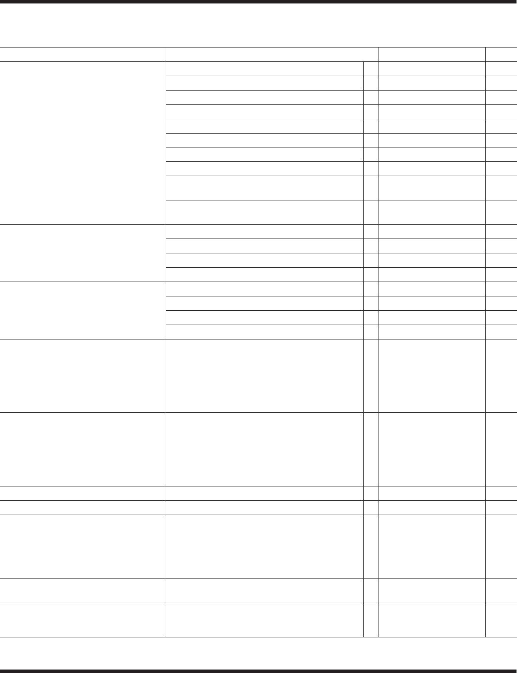
PARAMETER CONDITIONS MIN TYP MAX UNITS
Quiescent Current in Shutdown V
INP
= 6V, V
SHDNP
= 0V, V
INN
= 0V
V
INN
= –6V, V
SHDNN
= 0V, V
INP
= 0V (LT3032, LT3032-3.3,
LT3032-5)
V
INN
= V
OUT(NOMINAL)
–1V, V
SHDNN
= 0V, V
INP
= 0V
(LT3032-12/ LT3032-15)
l
l
l
0.1
–3
10
8
–10
20
µA
µA
µA
Output V
oltage Noise (10Hz to 100kHz) C
OUTP
= 10µF, C
BYPP
0.01µF, I
LOAD
= 150mA
C
OUTN
= 10µF, C
BYPN
0.01µF, I
LOAD
= –150mA
20
30
µV
RMS
µV
RMS
Ripple Rejection
V
RIPPLE
= 0.5V
P-P,
f
RIPPLE
= 120Hz
V
INP
to V
OUTP
= 1.5V (Average), I
LOAD
= 100mA
V
INN
to V
OUTN
= –1.5V (Average), I
LOAD
= –100mA
50
46
68
54
dB
dB
Current Limit (Note 12) V
INP
= 7V, V
OUTP
= 0V
V
INN
= –7V, V
OUTN
= 0V
V
INP
= 2.3V or V
OUTP(NOMINAL)
+ 1V, ΔV
OUTP
= –0.1V
V
INN
= –2.3V or V
OUTP(NOMINAL)
– 1V, ΔV
OUTN
= 0.1V
l
l
170
170
400
350
mA
mA
mA
mA
INP Reverse Leakage Current V
INP
= –20V, V
OUTP
= 0V
l
–1 mA
INN Reverse Leakage Current V
INN
= 20V, V
OUTN
, V
ADJN
, V
SHDNN
= Open Circuit
l
1 mA
Reverse Output Current
(Notes 5, 11)
LT3032-3.3
LT3032-5
LT3032-12
LT3032-15
LT3032
V
OUTP
= 3.3V, V
INP
< 3.3V
V
OUTP
= 5V, V
INP
< 5V
V
OUTP
= 12V, V
INP
< 12V
V
OUTP
= 15V, V
INP
< 15V
V
OUTP
= V
ADJP
= 1.22V, V
INP
< 1.22V
10
10
25
25
5
20
20
50
50
10
µA
µA
µA
µA
µA