LTC201A/LTC202/LTC203
4
201a23fb
LTC201AM/LTC202M/ LTC201AC/LTC202C/
LTC203M LTC203C
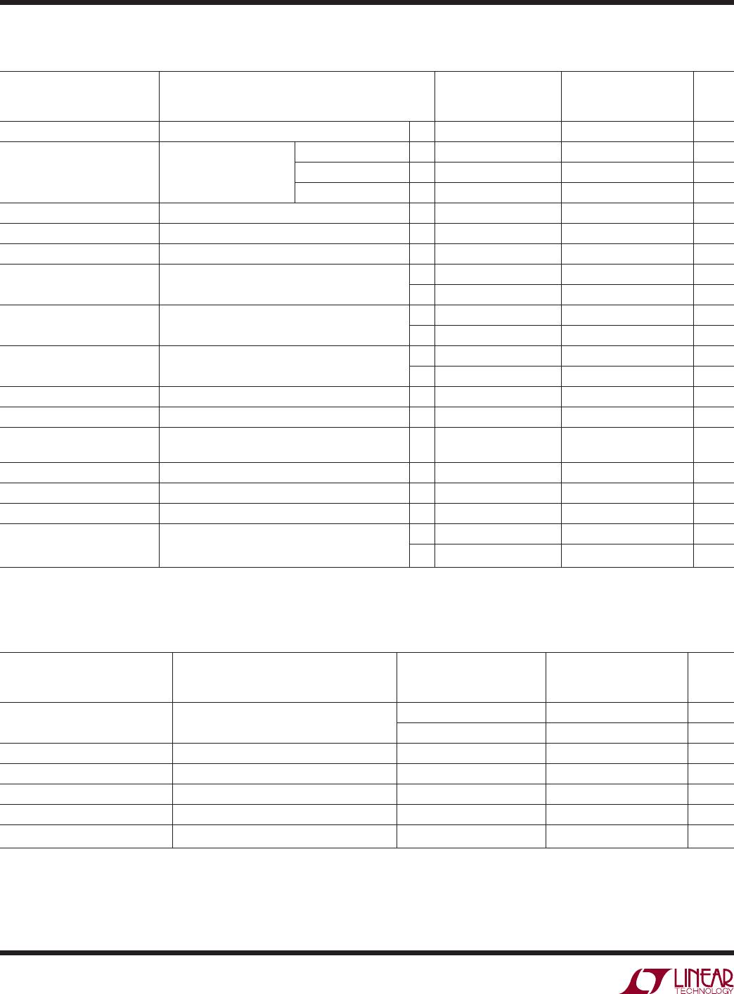
PARAMETER CONDITIONS MIN TYP MAX MIN TYP MAX UNITS
t
ON
V
S
= 2V, R
L
= 1kΩ, C
L
= 35pF 450 600 450 600 ns
t
OFF
190 300 190 300 ns
t
OPEN
100 250 100 250 ns
Off Isolation V
S
= 2V
P-P
, R
L
= 1kΩ, f = 100Hz 75 75 dB
Crosstalk 90 90 dB
Charge Injection O
INJ
R
S
= 0Ω, C
L
= 1000pF, V
S
= 2.5V 2 2 pC
Total Harmonic Distortion THD V
S
= 2V
P-P
, R
L
= 10kΩ 0.01 0.01 %
The ● denotes the specifications which
apply over full operating temperature range, otherwise specifications are at T
A
= 25°C. V
+
= 5V, V
–
= GND = 0V unless otherwise noted.
AC ELECTRICAL CHARACTERISTICS
DIGITAL A D DC ELECTRICAL CHARACTERISTICS
U
LTC201AM/LTC202M/ LTC201AC/LTC202C/
LTC203M LTC203C
PARAMETER CONDITIONS MIN TYP MAX MIN TYP MAX UNITS
Analog Signal Range ● 0505V
R
ON
V
S
= ±1.5V, +3V T
MIN
450 520 Ω
I
D
= 0.25mA 25°C 280 450 280 525 Ω
T
MAX
650 650 Ω
∆R
ON
vs V
S
20 20 %
∆R
ON
vs Temperature 0.5 0.5 %/°C
∆R
ON
Match V
S
= 2.5V, I
DS
= 0.25mA 5 5 %
Off Input Leakage I
S
(OFF) V
D
= 4V, 1V; V
S
= 1V, 4V (Note 4) 0.01 ±1 0.01 ±5nA
Switch Off ● ±100 ±100 nA
Off Output Leakage I
D
(0FF) V
D
= 4V, 1V; V
S
= 1V, 4V (Note 4) 0.01 ±1 0.01 + 5 nA
Switch Off ● ±100 ±100 nA
On Channel Leakage l
D
(ON) V
D
= V
S
= 1V, 4V (Note 4) 0.01 ±1 0.01 ±5nA
Switch On ● ±200 ±200 nA
Input High Voltage V
INH
● 2.4 2.4 V
Input Low Voltage V
INL
● 0.8 0.8 V
Input High or Low Current V
IN
= 5V, 0V ● ±1 ±1 µA
I
INH
and I
INL
C
S
(OFF) 55pF
C
D
(OFF) 12 12 pF
C
D
, C
S
(ON) 30 30 pF
I
+
All Logic Inputs Tied Together 8 20 8 20 µA
V
IN
= 0V OR 4.0V ● 30 30 µA
V
+
= 5V, V
–
= GND = 0V unless otherwise noted.
Note 1: Absolute Maximum Ratings are those values beyond which the life
of a device may be impaired.
Note 2: Signals on S, D, or IN exceeding V
+
or V
–
will be clamped by
internal diodes. Limit forward diode current to maximum current rating.
Note 3: In-circuit ESD on the switch pins (S or D) exceeds 4kV (see test
circuit).
Note 4: Leakage current with a single 5V supply is guaranteed by
correlation with the ±15V leakage current.