10
LTC1562-2
15622fa
Because 2nd order sections with Q ≥ 1 have response
peaks near f
O
, the gain ratio above implies some rules of
thumb:
f
O
< 200kHz ⇒ V2 tends to have the larger swing
f
O
> 200kHz ⇒ V1 tends to have the larger swing.
The following situations are convenient because the
relative swing issue does not arise. The unused output’s
swing is naturally the smaller of the two in these cases:
Lowpass response (resistor input, V2 output, Figure 5)
with f
O
< 200kHz
Bandpass response (capacitor input, V2 output, Figure
6b) with f
O
< 200kHz
Bandpass response (resistor input, V1 output, Figure
6a) with f
O
> 200kHz
Highpass response (capacitor input, V1 output, Figure
7) with f
O
> 200kHz
The LTC1562, a lower frequency variant of the LTC1562 -2,
has a design center f
O
of 100kHz compared to 200kHz in the
LTC1562-2. The rules summarized above apply to the
LTC1562 but with 100kHz replacing the 200kHz limits.
Thus, an LTC1562 highpass filter section with f
O
above
100kHz automatically satisfies the desirable condition of the
unused output carrying the smaller signal swing.
require further dynamic range, reducing the value of Z
IN
boosts the signal gain while reducing the input referred
noise. This feature can increase the SNR for low level
signals. Varying or switching Z
IN
is also an efficient way to
effect automatic gain control (AGC). From a system view-
point, this technique boosts the ratio of maximum signal
to minimum noise, for a typical 2nd order lowpass re-
sponse (Q = 1, f
O
= 200kHz), to 114dB.
Input Voltages Beyond the Power Supplies
Properly used, the LTC1562-2 can accommodate input
voltage excursions well beyond its supply voltage. This
requires care in design but can be useful, for example,
when large out-of-band interference is to be removed from
a smaller desired signal. The flexibility for different input
voltages arises because the INV inputs are at virtual
ground potential, like the inverting input of an op amp with
negative feedback. The LTC1562-2 fundamentally responds
to input
current
and the external voltage V
IN
appears only
across the external impedance Z
IN
in Figure 3.
To accept beyond-the-supply input voltages, it is impor-
tant to keep the LTC1562-2 powered on, not in shutdown
mode, and to avoid saturating the V1 or V2 output of the
2nd order section that receives the input. If any of these
conditions is violated, the INV input will depart from a
virtual ground, leading to an overload condition whose
recovery timing depends on circuit details. In the event
that this overload drives the INV input beyond the supply
voltages, the LTC1562-2 could be damaged.
The most subtle part of preventing overload is to consider
the possible input signals or spectra and take care that
none of them can drive either V1 or V2 to the supply limits.
Note that neither output can be allowed to saturate, even
if it is not used as the signal output. If necessary the
passband gain can be reduced (by increasing the imped-
ance of Z
IN
in Figure 3) to reduce output swings.
The final issue to be addressed with beyond-the-supply
inputs is current and voltage limits. Current entering the
virtual ground INV input flows eventually through the
output circuitry that drives V1 and V2. The input current
magnitude (V
IN
/Z
IN
in Figure 3) should be limited by
design to less than 1mA for good distortion performance.
On the other hand, the input voltage V
IN
appears across the
APPLICATIONS INFORMATION
WUU
U
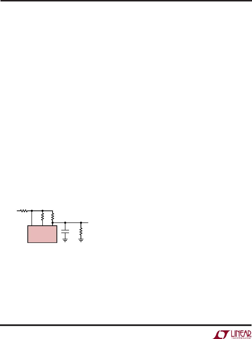
INV V1
2nd ORDER
1/4 LTC1562-2
V2
1562-2 F08
R2
7.87k
C
L
30pF
R
L
(EXTERNAL
LOAD RESISTANCE)
R
Q
5.49k
R
IN
7.87k
V
IN
V
OUT
Figure 8. 200kHz, Q = 0.7 Lowpass Circuit
for Distortion vs Loading Test
Low Level or Wide Range Input Signals
The LTC1562-2 contains a built-in capability for low noise
amplification of low level signals. The Z
IN
impedance in
each 2nd order section controls the block’s gain. When set
for unity passband gain, a 2nd order section can deliver an
output signal 99dB above the noise level. If low level inputs