3
DEMO MANUAL DC247
DESIGN-READY SWITCHER
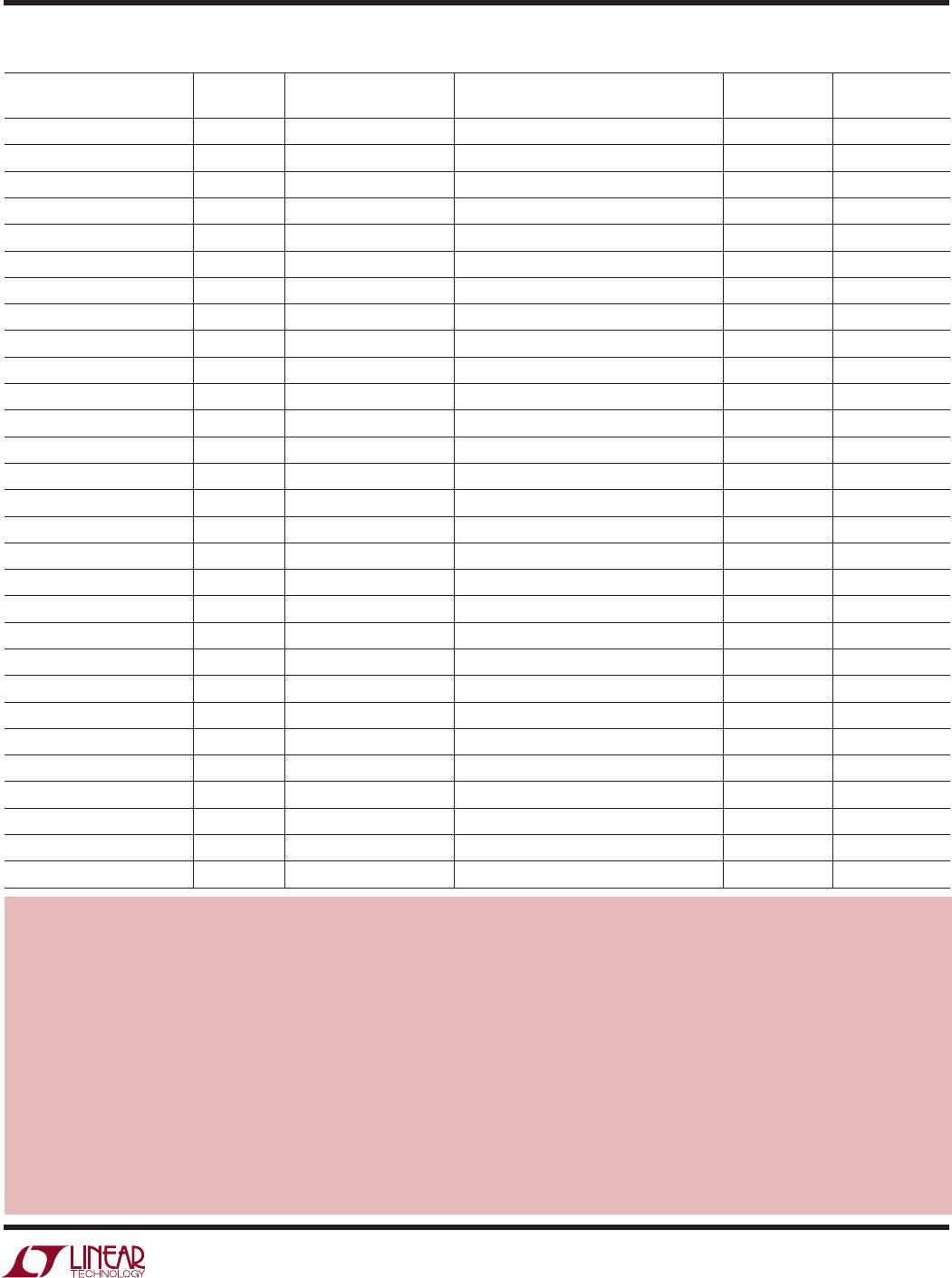
PARTS LIST
CF1, C
SS1
2 08055A104KAT1A 0.1µF 50V 20% X7R Capacitor AVX (843) 946-0362
C
IN1
, C
IN2
2 30SC22M 22µF 30V OS-CON Capacitor SANYO (619) 661-6835
C
IN3
, C
IN4
ALTERNATE THCR70E1H2262T 22µF 50V 20% Y5U Capacitor Marcon (847) 696-2000
CO1, CO2, CO4 ALTERNATE TS10X4470JAT1A 470µF 6.3V Low ESR Capacitor Kemet (408) 986-0424
CO1, C02, C04 ALTERNATE EEFUE0G181R 180µF 4V SP Capacitor Panasonic (201) 348-7522
CO3 1 4SP820M 820µF 4V OS-CON Capacitor SANYO (619) 661-6835
CO2 1 EEFCD0D101R 100µF 2V SP Capacitor Panasonic (201) 348-7522
C
OSC1
1 08055A470JAT1A 47pF 50V 5% NPO Capacitor AVX (843) 946-0362
C
S1
1 08055A102MAT1A 1000pF 50V 5% NPO Capacitor AVX (843) 946-0362
C4 1 0805ZC105MAT1A 1µF 10V 20% X7R Capacitor AVX (843) 946-0362
D1 1 CMDSH-3 0.1A BVR = 30V Schottky Diode Central (516) 435-1110
D2 1 MBRS340T3 3A BVR = 40V Schottky Diode Motorola (800) 441-2447
E2, E3, E4, E7–E10 7 1502-2 Turret Terminal Keystone (718) 956-8900
JP1 1 2802S-03-G2 2mm Pin Header Comm Con (626) 301-4200
JP2 1 2802S-02-G2 2mm Pin Header Comm Con (626) 301-4200
L1 1 ETQP6F2ROHFA 2µH Inductor Panasonic (201) 348-7522
M1, M2 2 FDS6680A 0.013Ω 30V N-Channel MOSFET Fairchild (408) 822-2126
Q1 OPTIONAL VN2222 10Ω 20V N-Channel MOSFET
R1 OPTIONAL CR16-103JM 10k 1/10W 5% Chip Resistor TAD (800) 508-1521
R2, R5, R
S1
3 CR16-100FM 10Ω 1/10W 1% Chip Resistor TAD (800) 508-1521
R3, R7 2 W0805-03-1002B 10k 1/10W 0.1% Chip Resistor IRC (361) 992-7900
R4 OPTIONAL USER DEF 1/10W 1% Chip Resistor
R6 1 CR16-684JM 680k 1/10W 5% Chip Resistor TAD (800) 508-1521
R8 1 CR16-000M 0Ω 1/10W Chip Resistor TAD (800) 508-1521
R
C1
1 CR16-333FM 33k 1/10W 5% Chip Resistor TAD (800) 508-1521
R
CS1
1 LRF2010-01-R005J 0.005Ω 1W 5% Resistor IRC (512) 992-7900
RF1 1 CR16-470JM 4.7Ω 1/10W 5% Chip Resistor TAD (800) 508-1521
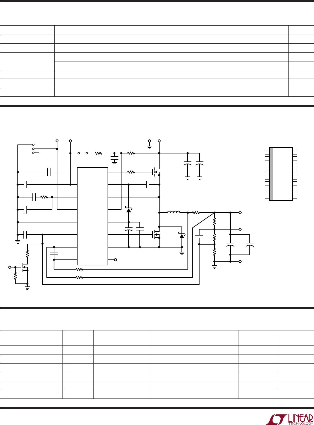
U1 1 LTC1735CS16 IC, Switching Regulator Controller LTC (408) 432-1900
2 CCIJ2mm-138-G Jumper Comm Con (626) 301-4200
REFERENCE
DESIGNATOR QUANTITY PART NUMBER DESCRIPTION VENDOR TELEPHONE
QUICK START GUIDE
This demonstration board is easily set up to evaluate the
performance of the LTC1735. Please follow the proce-
dure outlined below for proper operation. Soldered wire
connections are required to properly ascertain the per-
formance of this switching regulator.
• Refer to Figure 2 for proper connection of monitoring
and measurement equipment.
• Connect the input power supply to the V
IN
and GND
terminals on the right hand side of the board with
soldered connections. Do not increase V
IN
over 28V or
the MOSFET(s) WILL BE DAMAGED.
• Connect the load between the V
OUT
and GND terminals
on the right side of the board with soldered connec-
tions.
• The RUN pin can be left unconnected. To shut down
the LTC1735, tie this pin to ground.
• If an external 5V supply is used, connect it to EXTV
CC
.