MMBF170LT1G

© Semiconductor Components Industries, LLC, 1994
October, 2016 Rev. 10
1 Publication Order Number:
MMBF170LT1/D
MMBF170L, NVBF170L
Power MOSFET
500 mA, 60 V, NChannel SOT23
Features
NVBF Prefix for Automotive and Other Applications Requiring
Unique Site and Control Change Requirements; AECQ101
Qualified and PPAP Capable
These Devices are PbFree and are RoHS Compliant
MAXIMUM RATINGS
Rating Symbol Value Unit
DrainSource Voltage V
DSS
60 Vdc
DrainGate Voltage V
DGS
60 Vdc
GateSource Voltage
Continuous
Nonrepetitive (t
p
50 ms)
V
GS
V
GSM
± 20
± 40
Vdc
Vpk
Drain Current Continuous
Pulsed
I
D
I
DM
0.5
0.8
Adc
THERMAL CHARACTERISTICS
Characteristic Symbol Max Unit
Total Device Dissipation FR 5 Board
(Note 1.) T
A
= 25°C
Derate above 25°C
P
D
225
1.8
mW
mW/°C
Thermal Resistance, JunctiontoAmbient
R
q
JA
556 °C/W
Junction and Storage Temperature T
J
, T
stg
55 to
+150
°C
Stresses exceeding those listed in the Maximum Ratings table may damage the
device. If any of these limits are exceeded, device functionality should not be
assumed, damage may occur and reliability may be affected.
1. FR5 = 1.0 0.75 0.062 in.
3
1
2
NChannel
SOT23
CASE 318
STYLE 21
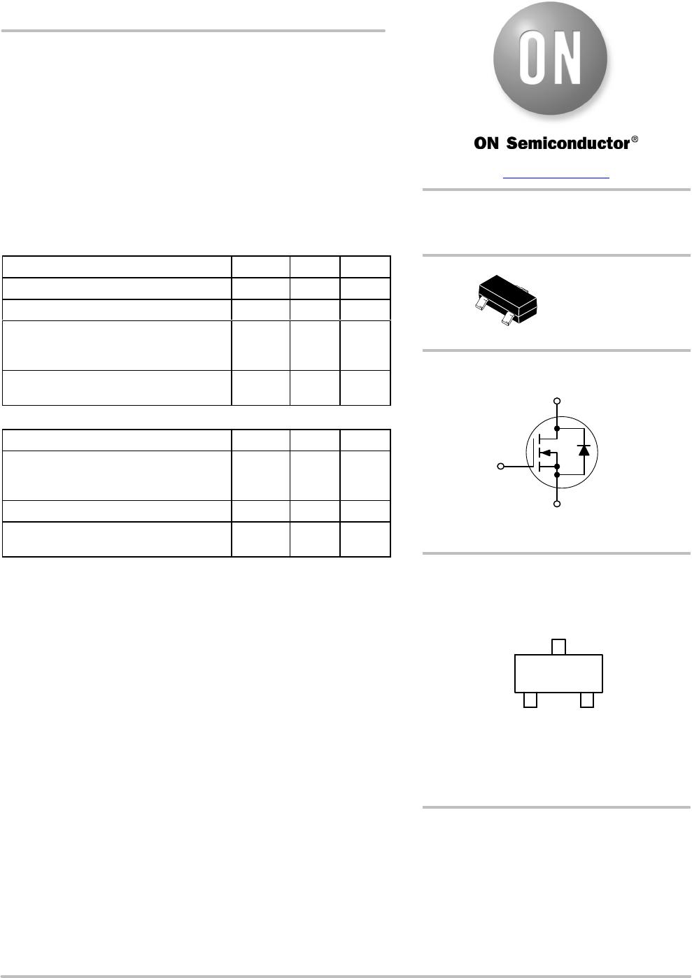
MARKING DIAGRAM
& PIN ASSIGNMENT
500 mA, 60 V
R
DS(on)
= 5 W
3
Drain
2 SourceGate 1
www.onsemi.com
ORDERING INFORMATION
See detailed ordering and shipping information in the
package dimensions section on page 2 of this data sheet.
6Z MG
G
6Z = Specific Device Code
M = Date Code
G = PbFree Package
(Note: Microdot may be in either location)
MMBF170L, NVBF170L
www.onsemi.com
2
ELECTRICAL CHARACTERISTICS (T
C
= 25°C unless otherwise noted)
Characteristic
Symbol Min Max Unit
OFF CHARACTERISTICS
DrainSource Breakdown Voltage (V
GS
= 0, I
D
= 100 mA)
V
(BR)DSS
60 Vdc
GateBody Leakage Current, Forward (V
GSF
= 15 Vdc, V
DS
= 0) I
GSS
10 nAdc
ON CHARACTERISTICS (Note 1)
Gate Threshold Voltage (V
DS
= V
GS
, I
D
= 1.0 mA) V
GS(th)
0.8 3.0 Vdc
Static DrainSource OnResistance (V
GS
= 10 Vdc, I
D
= 200 mA) r
DS(on)
5.0
W
OnState Drain Current (V
DS
= 25 Vdc, V
GS
= 0) I
D(off)
0.5
mA
DYNAMIC CHARACTERISTICS
Input Capacitance
(V
DS
= 10 Vdc, V
GS
= 0 V, f = 1.0 MHz)
C
iss
60 pF
SWITCHING CHARACTERISTICS (Note 1)
TurnOn Delay Time
(V
DD
= 25 Vdc, I
D
= 500 mA, R
gen
= 50 W)
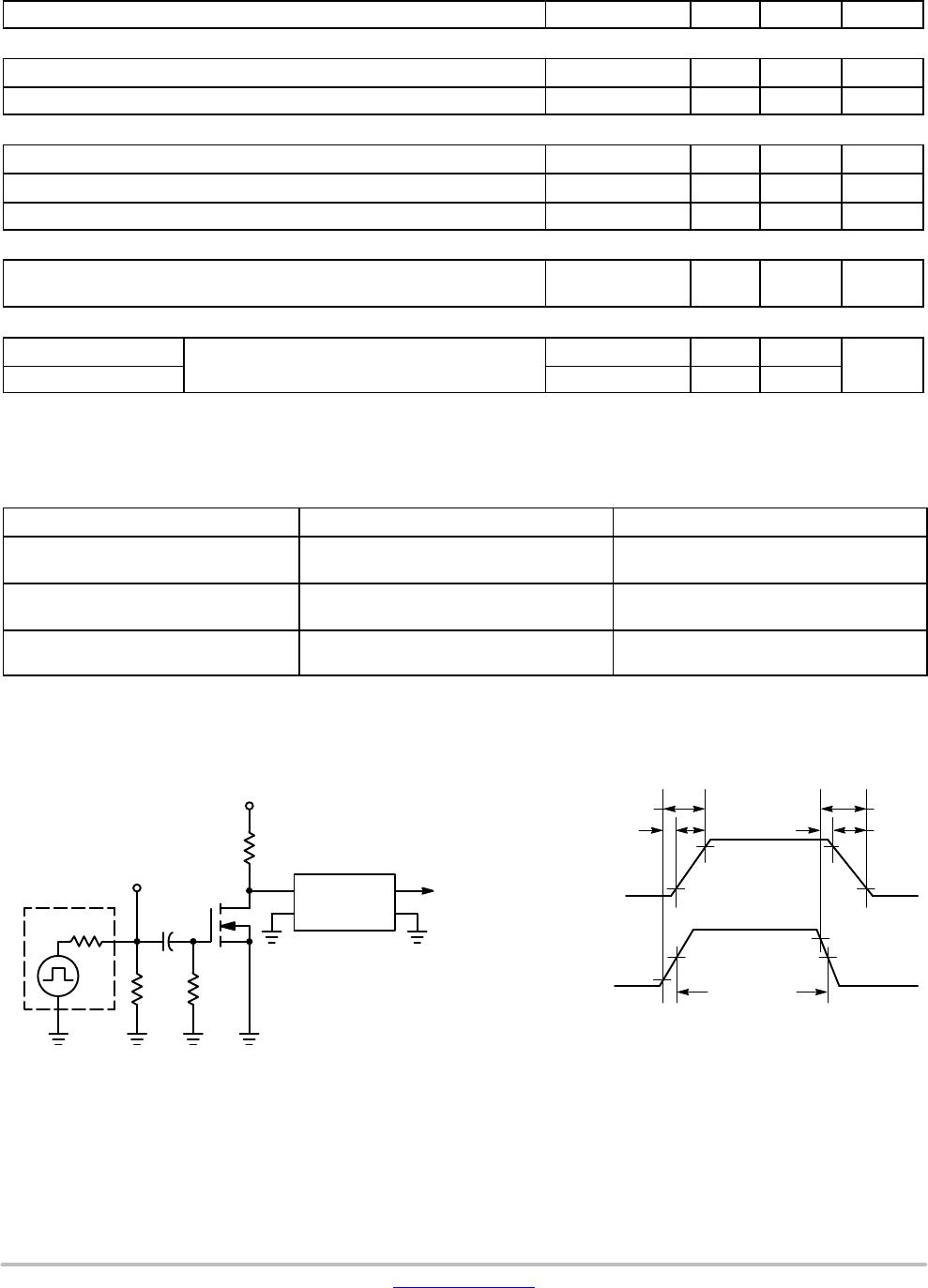
Figure 1
t
d(on)
10
ns
TurnOff Delay Time t
d(off)
10
Product parametric performance is indicated in the Electrical Characteristics for the listed test conditions, unless otherwise noted. Product
performance may not be indicated by the Electrical Characteristics if operated under different conditions.
1. Pulse Test: Pulse Width v 300 ms, Duty Cycle v 2.0%.
ORDERING INFORMATION
Device Package Shipping
MMBF170LT1G SOT23 (TO236)
(PbFree)
3000 / Tape & Reel
MMBF170LT3G SOT23 (TO236)
(PbFree)
10000 / Tape & Reel
NVBF170LT1G* SOT23 (TO236)
(PbFree)
3000 / Tape & Reel
For information on tape and reel specifications, including part orientation and tape sizes, please refer to our Tape and Reel Packaging
Specifications Brochure, BRD8011/D.
Figure 1. Switching Test Circuit Figure 2. Switching Waveform
20 dB 50 W
ATTENUATOR
PULSE
GENERATOR
50 W
50 W 1 MW
V
out
125 W
+25 V
40 pF
V
in
TO SAMPLING
SCOPE
50 W INPUT
PULSE WIDTH
50%
90%
50%
10%
10%
90%
90%
V
in
OUTPUT
INVERTED
INPUT
(V
in
AMPLITUDE 10 VOLTS)
V
out
t
off
t
f
t
d(off)
t
on
t
d(on)
t
r
MMBF170L, NVBF170L
www.onsemi.com
3
TYPICAL ELECTRICAL CHARACTERISTICS
Figure 3. OnRegion Characteristics Figure 4. Transfer Characteristics
V
DS
, DRAINTOSOURCE VOLTAGE (V) V
GS
, GATETOSOURCE VOLTAGE (V)
7543210
0
0.2
0.4
0.6
0.8
4321
0
0.4
0.8
1.0
I
D
, DRAIN CURRENT (A)
I
D
, DRAIN CURRENT (A)
1.0
1.2
T
J
= 25°C
V
GS
= 10 V
4.2 V
5.0 V
4.5 V
4.0 V
3.8 V
3.6 V
3.4 V
3.2 V
3.0 V
2.8 V
V
DS
10 V
T
J
= 25°C
T
J
= 150°C
T
J
= 55°C
0.2
0.6
Figure 5. OnResistance vs. Drain Current and
Gate Voltage
I
D
, DRAIN CURRENT (A)
0.850.550.450.350.250.15
0
1
2
3
4
5
R
DS(on)
, DRAINTOSOURCE RESISTANCE (W)
0.65 0.75
T
J
= 25°C
V
GS
= 4.5 V
V
GS
= 10 V
Figure 6. GatetoSource and
DraintoSource Voltage vs. Total Charge
Q
g
, TOTAL GATE CHARGE (nC)
10.50
0
2.5
5
12.5
15
V
GS
, GATETOSOURCE VOLTAGE (V)
1.5
10
7.5
V
DS
, DRAINTOSOURCE VOLTAGE (V)
30
25
15
10
5
0
I
D
= 0.5 A
T
J
= 25°C
QT
V
DS
V
GS
Q
gd
Q
gs
Figure 7. Diode Forward Voltage vs. Current
V
SD
, SOURCETODRAIN VOLTAGE (V)
0.90.80.70.60.50.4
0
0.04
0.20
I
S
, SOURCE CURRENT (A)
0.08
0.12
0.16
0.24
V
GS
= 0 V
T
J
= 25°C
6
7
8
2
20
0.02
0.06
0.22
0.10
0.14
0.18
1.00.30.20.1
8765
6

MMBF170LT1G

Mfr. #:
Manufacturer:
ON Semiconductor
Description:
MOSFET 60V 500mA N-Channel
Lifecycle:
New from this manufacturer.
Delivery:
DHL FedEx Ups TNT EMS
Payment:
T/T Paypal Visa MoneyGram Western Union

Products related to this Datasheet