Design and specifications are each subject to change without notice. Ask factory for the current technical specifications before purchase and/or use.
Should a safety concern arise regarding this product, please be sure to contact us immediately.
Chip Resistor Networks
I03
0.3±0.2
0.5±0.2
f0.3
+0.1
–0.2
0.3±0.2
0.25±0.20
0.5±0.2
0.8±0.1
4.0±0.2
0.25±0.20
0.35±0.20
0.4±0.2
0.35±0.20
0.4±0.2
0.5±0.2
0.4±0.2
2.1±0.2
0.55±0.10
f0.3
+0.1
–0.2
0.7±0.2
0.3±0.2
0.3±0.2
6.4±0.2
1.27±0.10
0.5±0.2
0.5±0.2
0.5±0.2
3.1±0.2
0.55±0.10
I03
EXBA10E
I03
I03
EXBA10P
0.25±0.10
0.3±0.1
0.25±0.10
0.35±0.15
0.35
±
0.15
0.40±0.15
1.60±0.15
0.55±0.10
0.2±0.1
0.33±0.15
0.2±0.1
0.2±0.1
0.2
±
0.1
f0.2±0.1
3.20±0.15
0.635±0.10
0.40±0.15
0.15
+0.15
–0.05
0.15
+0.20
–0.05
0.15
+0.15
–0.05
0.3±0.1
0.2±0.1
0.25±0.15
3.8±0.2
0.5±0.1
0.30±0.15
1.6±0.2
0.45±0.10
472
10987
2345
61
10 6
15
987
234
10 6
15
987
234
10
15
9
234
678
111213141516
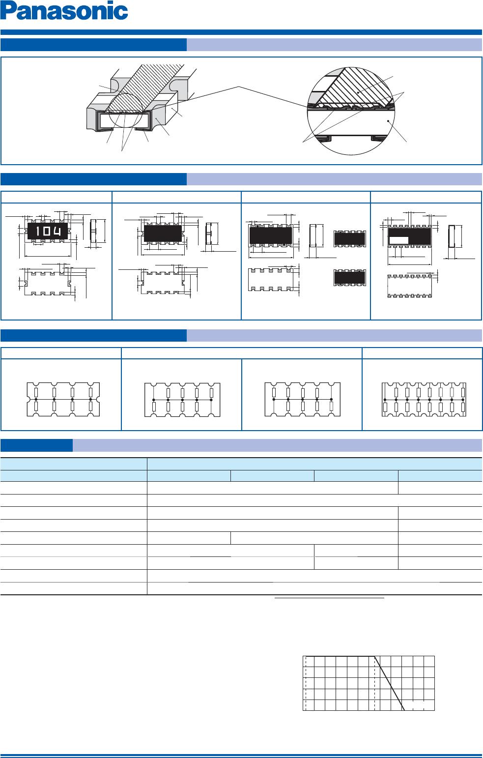
Protective coating
Thick film
resistive element
Electrode (Inner)
Electrode (Between)
Electrode (Outer)
Alumina substrate
Alumina substrate
Protective coating
Electrode
(Inner)
Thick film
resistive element
0
20
40
60
80
100
–60 –40 –20
0 20406080
100120140160180
–55 °C 70 °C
125 °C
Rated Load (%)
Ambient Temperature (°C)
Construction (Example : EXBD)
Dimensions in mm (not to scale)
Circuit Con guration
Power Derating Curve
For resistors operated in ambient temperatures above
70 °C, power rating shall be derated in accordance
with the figure on the right.
Ratings
EXBD EXBE EXBA EXBQ
Mass (Weight)[1000 pcs.] : 10 g
Mass (Weight)[1000 pcs.] : 16 g Mass (Weight)[1000 pcs.] : 40 g
Mass (Weight)[1000 pcs.] : 9 g
EXBD, EXBE EXBA EXBQ
Item Specifi cations
Series EXBD EXBE EXBA EXBQ
Resistance Range 47 Ω to 1 MΩ (E12)
100 Ω to 470 kΩ (E6 series)
Resistance Tolerance ±5%
Number of Terminals 10 terminals 16 terminals
Number of Resistors 8 element 15 element
Power Rating at 70 °C 0.05 W/element 0.063 W/element 0.025 W/element
Limiting Element Voltage
(1)
25V 50 V 25V
Maximum Overload Voltage
(2)
50 V 100 V 50 V
T. C. R. ±200 × 10
–6
/ °C
Category Temperature Range
–55 °C to +125 °C
EXBA10P
EXBA10E
(1) Rated Continuous Working Voltage (RCWV) shall be determined from RCWV=
√
Power Rating × Resistance Value, or Limiting Element Voltage
listed above, whichever less.
(2) Overload (Short-time Overload) Test Voltage (SOTV) shall be determinedfrom SOTV=2.5 × RCWV
✽
or Maximum Overload Voltage list ed above
which ev er less.
Sep. 201402
