ADuM120N/ADuM121N Data Sheet
Rev. B | Page 4 of 19
Parameter Symbol Min Typ Max Unit Test Conditions/Comments
AC SPECIFICATIONS
Output Rise/Fall Time t
R
/t
F
2.5 ns 10% to 90%
Common-Mode Transient
Immunity
6
|CM
H
| 75 100 kV/µs V
Ix
= V
DDx
, V
CM
= 1000 V, transient
magnitude = 800 V
|CM
L
| 75 100 kV/µs V
Ix
= 0 V, V
CM
= 1000 V, transient
magnitude = 800 V
1
I
Ox
is the Channel x output current, where x = A or B.
2
V
IxH
is the input side logic high voltage.
3
V
IxL
is the input side logic low voltage.
4
V
I
is the input voltage.
5
N0 is the ADuM120N0/ADuM121N0 models, and N1 is the ADuM120N1/ADuM121N1 models. See the Ordering Guide.
6
|CM
H
| is the maximum common-mode voltage slew rate that can be sustained while maintaining the voltage output (V
O
) > 0.8 V
DDx
. |CM
L
| is the maximum common-
mode voltage slew rate that can be sustained while maintaining V
O
> 0.8 V. The common-mode voltage slew rates apply to both rising and falling common-mode
voltage edges.
Table 2. Total Supply Current vs. Data Throughput
1 Mbps 25 Mbps 100 Mbps
Parameter Symbol Min Typ Max Min Typ Max Min Typ Max Unit
SUPPLY CURRENT
ADuM120N
Supply Current Side 1 I
DD1
3.7 6.8 4.2 7.2 6.2 9.3 mA
Supply Current Side 2 I
DD2
1.4 2.0 2.5 3.2 6.0 8.1 mA
ADuM121N
Supply Current Side 1
I
DD1
2.6
4.5
3.2
5.4
5.4
8.2
mA
Supply Current Side 2 I
DD2
3.0 4.9 3.7 5.9 5.8 8.6 mA
Data Sheet ADuM120N/ADuM121N
Rev. B | Page 5 of 19
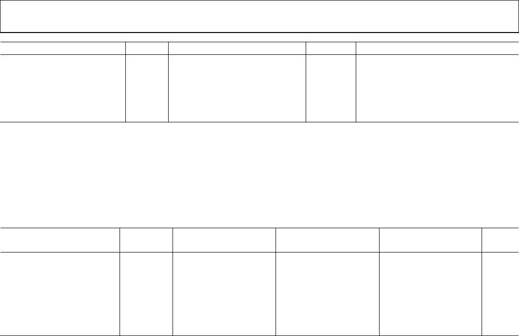
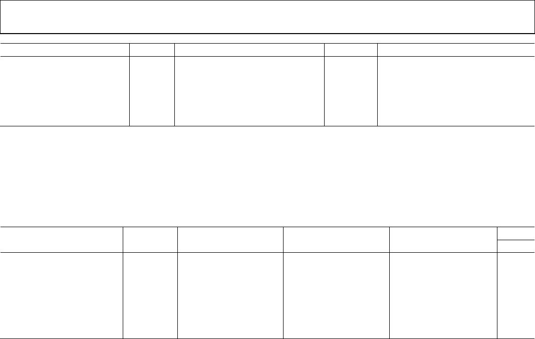
ELECTRICAL CHARACTERISTICS3.3 V OPERATION
All typical specifications are at T
A
= 25°C, V
DD1
= V
DD2
= 3.3 V. Minimum/maximum specifications apply over the entire recommended
operation range: 3.0 V ≤ V
DD1
≤ 3.6 V, 3.0 V ≤ V
DD2
3.6 V, and −40°C T
A
≤ +125°C, unless otherwise noted. Switching specifications
are tested with C
L
= 15 pF and CMOS signal levels, unless otherwise noted. Supply currents are specified with 50% duty cycle signals.
Table 3.
Parameter Symbol Min Typ Max Unit Test Conditions/Comments
SWITCHING SPECIFICATIONS
Pulse Width PW 6.6 ns Within PWD limit
Data Rate 150 Mbps Within PWD limit
Propagation Delay t
PHL
, t
PLH
4.8 6.8 14 ns 50% input to 50% output
Pulse Width Distortion PWD 0.7 3 ns |t
PLH
− t
PHL
|
Change vs. Temperature 1.5 ps/°C
Propagation Delay Skew t
PSK
7.0 ns Between any two units at the same
temperature, voltage, and load
Channel Matching
Codirectional t
PSKCD
0.7 3.0 ns
Opposing Direction t
PSKOD
0.7 3.0 ns
Jitter 290 ps p-p See the Jitter Measurement section
45 ps rms See the Jitter Measurement section
DC SPECIFICATIONS
Input Threshold Voltage
Logic High V
IH
0.7 × V
DDx
V
Logic Low V
IL
0.3 × V
DDx
V
Output Voltage
Logic High V
OH
V
DDx
− 0.1 V
DDx
V I
Ox
1
= −20 µA, V
Ix
= V
IxH
2
V
DDx
− 0.4 V
DDx
− 0.2 V I
Ox
1
= −2 mA, V
Ix
= V
IxH
2
Logic Low V
OL
0.0 0.1 V I
Ox
1
= 20 µA, V
Ix
= V
IxL
3
0.2 0.4 V I
Ox
1
= 2 mA, V
Ix
= V
IxL
3
Input Current per Channel
I
I
−10
+0.01
+10
µA
0 V ≤ V
Ix
V
DDx
Quiescent Supply Current
ADuM120N I
DD1 (Q)
0.8 1.3 mA V
I
4
= 0 (N0), 1 (N1)
5
I
DD2 (Q)
1.2 1.8 mA V
I
4
= 0 (N0), 1 (N1)
5
I
DD1 (Q)
6.3 9.7 mA V
I
4
= 1 (N0), 0 (N1)
5
I
DD2 (Q)
1.3 1.8 mA V
I
4
= 1 (N0), 0 (N1)
5
ADuM121N I
DD1 (Q)
1.0 1.6 mA V
I
4
= 0 (N0), 1 (N1)
5
I
DD2 (Q)
1.0 1.5 mA V
I
4
= 01 (N0), 1 (N1)
5
I
DD1 (Q)
3.9 5.8 mA V
I
4
= 1 (N0), 0 (N1)
5
I
DD2 (Q)
4.8 6.4 mA V
I
4
= 1 (N0), 0 (N1)
5
Dynamic Supply Current
Dynamic Input I
DDI (D)
0.01 mA/Mbps Inputs switching, 50% duty cycle
Dynamic Output
I
DDO (D)
0.01
mA/Mbps
Inputs switching, 50% duty cycle
Undervoltage Lockout UVLO
Positive V
DDx
Threshold V
DDxUV+
1.6 V
Negative V
DDx
Threshold V
DDxUV−
1.5 V
V
DDx
Hysteresis V
DDxUVH
0.1 V
ADuM120N/ADuM121N Data Sheet
Rev. B | Page 6 of 19
Parameter Symbol Min Typ Max Unit Test Conditions/Comments
AC SPECIFICATIONS
Output Rise/Fall Time t
R
/t
F
2.5 ns 10% to 90%
Common-Mode Transient
Immunity
6
|CM
H
| 75 100 kV/µs V
Ix
= V
DDx
, V
CM
= 1000 V, transient
magnitude = 800 V
|CM
L
| 75 100 kV/µs V
Ix
= 0 V, V
CM
= 1000 V, transient
magnitude = 800 V
1
I
Ox
is the Channel x output current, where x = A or B.
2
V
IxH
is the input side logic high voltage.
3
V
IxL
is the input side logic low voltage.
4
V
I
is the input voltage.
5
N0 is the ADuM120N0/ADuM121N0 models, and N1 is the ADuM120N1/ADuM121N1 models. See the Ordering Guide.
6
|CM
H
| is the maximum common-mode voltage slew rate that can be sustained while maintaining V
O
> 0.8 V
DDx
. |CM
L
| is the maximum common-mode voltage slew rate
that can be sustained while maintaining V
O
> 0.8 V. The common-mode voltage slew rates apply to both rising and falling common-mode voltage edges.
Table 4. Total Supply Current vs. Data Throughput
1 Mbps 25 Mbps 100 Mbps
Parameter Symbol Min Typ Max Min Typ Max Min Typ Max Unit
SUPPLY CURRENT
ADuM120N
Supply Current Side 1 I
DD1
3.6 6.2 4.0 6.7 5.6 9.1 mA
Supply Current Side 2 I
DD2
1.3 1.9 2.3 3.1 5.2 6.8 mA
ADuM121N
Supply Current Side 1 I
DD1
2.5 4.6 3.0 5.5 5.0 8.1 mA
Supply Current Side 2 I
DD2
2.9 4.8 3.5 5.8 5.4 8.3 mA

ADUM120N0BRZ-RL7

Mfr. #:
Manufacturer:
Analog Devices Inc.
Description:
Digital Isolators 2ch EMC robust 3kV digital Isolator 2/0
Lifecycle:
New from this manufacturer.
Delivery:
DHL FedEx Ups TNT EMS
Payment:
T/T Paypal Visa MoneyGram Western Union