NJU7024D
NJU7024M
NJU7024V
LOW VOLTAGE C-MOS OPERATIONAL AMPLIFIER
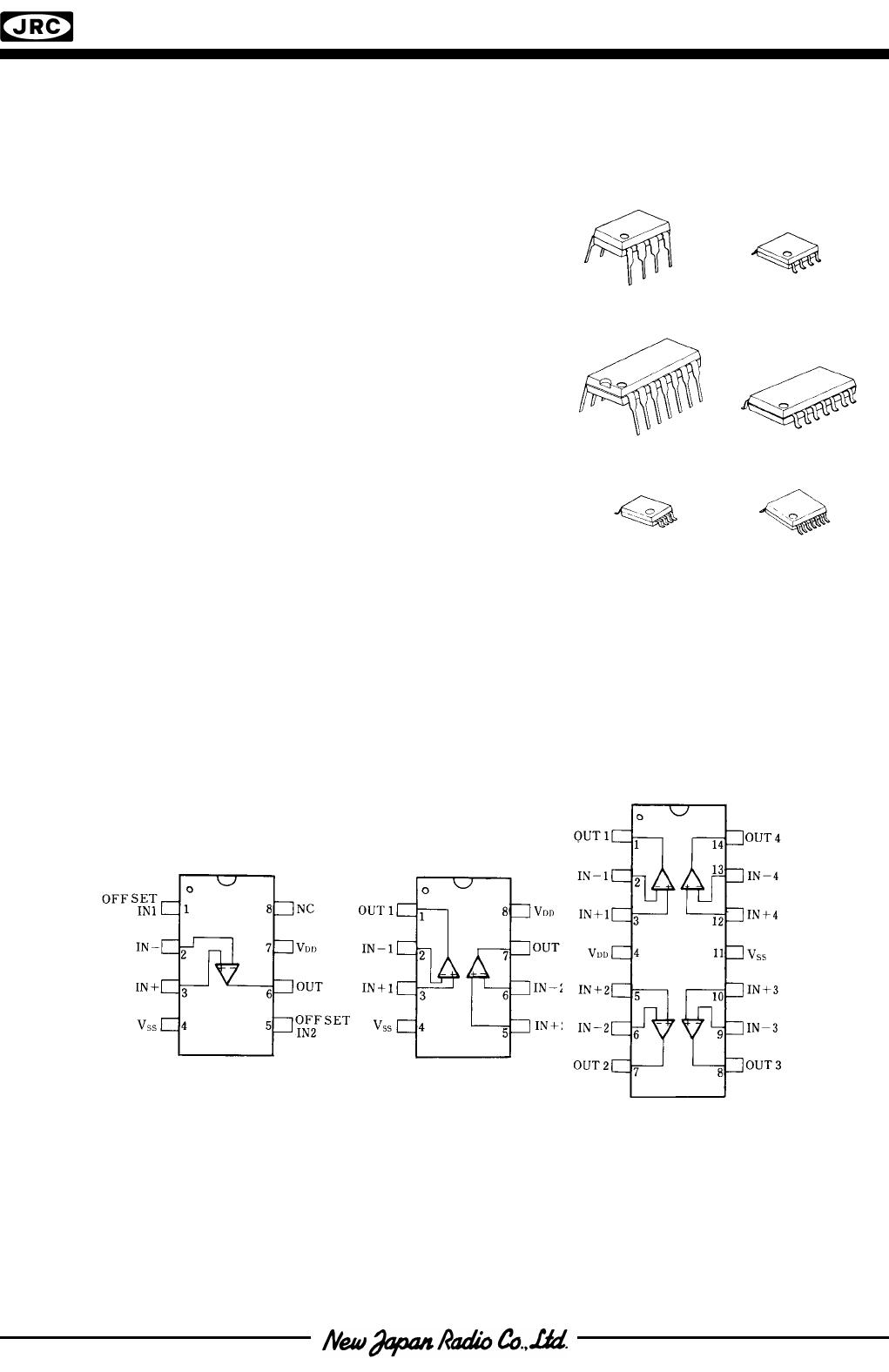
■ GENERAL DESCRIPTION ■ PACKAGE OUTLINE
The NJU7021,22 and 24 are single, dual and quad C-MOS
Operational Amplifiers operated on a single-power-supply, low
voltage and low operating current.
The minimum operating voltage is 3V and the output stage
permits output signals to swing between both of the supply rails.
The input bias current is as low as less than 1pA,consequently
the very small signal around the ground level can be amplified.
Furthermore, the operating current is also as low as 150μA
( typ ) per circuit, therefore it can be applied especially to battery
operated items.
■ FEATURES
● Single-Power-Supply
● Wide Operating Voltage ( V
DD
=3~16V )
● Wide Output Swing Range ( V
OM
=9.98V typ. @ V
DD
=10V )
● Low Operating Current ( 150μA/circuit )
● Low Bias Current ( I
IB
=1pA typ. )
● Internal Compensation Capacitor
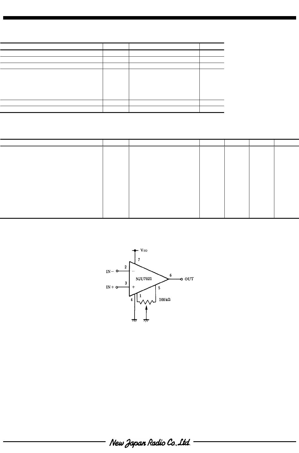
● External Offset Null Adjustment ( Only NJU7021 )
● Package Outline DMP/SSOP8 ( NJU7021 )
DIP/DMP8 ( NJU7022 )
DIP/DMP/SSOP14 ( NJU7024 )
● C-MOS Technology
■ PIN CONFIGURATION