© Semiconductor Components Industries, LLC, 2009
February, 2009 − Rev. 1
1 Publication Order Number:
NB7V585M/D
NB7V585M
1.8V / 2.5V Differential 2:1
Mux Input to 1:6 CML
Clock/Data Fanout
Buffer/Translator
Multi−Level Inputs w/ Internal Termination
Description
The NB7V585M is a differential 1−to−6 CML clock/data
distribution chip featuring a 2:1 Clock/Data input multiplexer with an
input select pin. The INx/INx
inputs incorporate internal 50 W
termination resistors and will accept LVPECL, CML, or LVDS logic
levels (see Figure 9). The NB7V585M produces six identical output
copies of clock or data operating up to 6 GHz or 10 Gb/s, respectively.
As such, NB7V585M is ideal for SONET, GigE, Fiber Channel,
Backplane and other clock/data distribution applications. The 16 mA
differential CML output structure provides matching internal 50 W
source terminations, 400 mV output swings when externally
terminated with a 50 W resistor to V
CC
(see Figure 14) and is
optimized for low skew and minimal jitter. The NB7V585M is
powered with either 1.8 V or 2.5 V supply and is offered in a low
profile 5x5 mm 32−pin QFN package.
Application notes, models, and support documentation are available
at www.onsemi.com.
The NB7V585M is a member of the GigaComm™ family of high
performance clock products.
Features
• Maximum Input Data Rate > 10 Gb/s
• Data Dependent Jitter < 10 ps
• Maximum Input Clock Frequency > 6 GHz
• Random Clock Jitter < 0.8 ps RMS, Max
• Low Skew 1:6 CML Outputs, 20 ps Max
• 2:1 Multi−Level Mux Inputs
• 175 ps Typical Propagation Delay
• 50 ps Typical Rise and Fall Times
• Differential CML Outputs, 330 mV Peak−to−Peak, Typical
• Operating Range: V
CC
= 1.71 V to 1.89 V
• Internal 50 W Input Termination Resistors
• V
REFAC
Reference Output
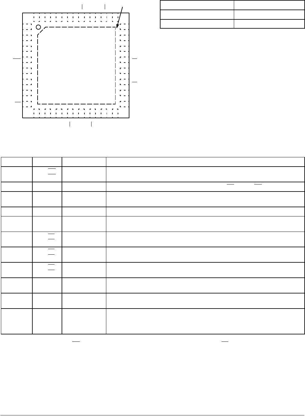
• QFN32 Package, 5 mm x 5 mm
• −40°C to +85°C Ambient Operating Temperature
• These are Pb−Free Devices
MARKING
DIAGRAM*
QFN32
MN SUFFIX
CASE 488AM
http://onsemi.com
*For additional marking information, refer to
Application Note AND8002/D.
See detailed ordering and shipping information in the package
dimensions section on page 7 of this data sheet.
ORDERING INFORMATION
SIMPLIFIED LOGIC DIAGRAM
32
1
NB7V
585M
AWLYYWW
G
1
A = Assembly Location
WL = Wafer Lot
YY = Year
WW = Work Week
G = Pb−Free Package
Q0
Q0
Q1
Q1
Q2
Q2
Q3
Q3
Q4
Q4
Q5
Q5
V
CC
SEL
V
REFAC0
IN0
VT0
IN0
IN1
VT1
IN1
V
REFAC1
V
CC
GND
0
1