DATASHEET
SPREAD SPECTRUM CLOCK SYNTHESIZER IDT5P50901/2/3/4
IDT®
SPREAD SPECTRUM CLOCK SYNTHESIZER 1
IDT5P50901/2/3/4 REV F 082112
Description
The IDT5P50901/2/3/4 is a family of 1.8V low power, spread
spectrum clock generators capable of reducing EMI
radiation from an input clock. Spread spectrum technique is
capable of reducing the harmonic frequency amplitude
peaks by several dB.
Ordering Information
Input Frequency
10 to 25 MHz - 5P50901NBGI/5P50901DVGI
20 to 50 MHz - 5P50902NBGI/5P50902DVGI
40 to 100 MHz - 5P50903NBGI/5P50903DVGI
80 to 170 MHz - 5P50904NBGI/5P50904DVGI
Features
8-pin DFN package (2x2mm)
8-pin MSOP package (3x4.9mm)
Provides a spread spectrum output clock
Input frequency range of 10 to 170 MHz
Output frequency range of 10 to 170 MHz
Center and down spread
Peak reduction by 8 dB to 16 dB typical on 3rd through
19th odd harmonics
Low EMI feature can be disabled
Operating voltage of 1.8 V, 2.5 or 3.3V
RoHS 6 compliant package
Spread Modulation Frequency Table
Block Diagram
Part
Number
Input
(MHz)
Modulation
(kHz)
Input
(MHz)
Modulation
(kHz)
Modulation
Frequency (kHz)
5P50901 10 27 25 67.5 ICLK*27/10000
5P50902 20 27 50 67.5 ICLK*27/20000
5P50903 40 27 100 67.5 ICLK*27/40000
5P50904 80 27 170 57.4 ICLK*27/80000
VDD
GND
ICLK
PLL Clock
Synthesizer with
Spread Spectrum
Circuitry
CLKOUT
2
S2:S0
IDT5P50901/2/3/4
SPREAD SPECTRUM CLOCK SYNTHESIZER CLOCK SYNTHESIZER
IDT®
SPREAD SPECTRUM CLOCK SYNTHESIZER 2
IDT5P50901/2/3/4 REV F 082112
Pin Assignment
Spread Direction and Percentage Select Table
Pin Description
S2 S1 S0 Spread
Direction
Spread
Percentage
000 OFF --
0 0 1 Center ±0.25
010 Center ±0.5
011 Center ±1.0
100 Center ±1.5
101 Center ±2.0
110 Down -0.5
111 Down -1.0
Pin
Number
Pin
Name
Pin Type Pin Description
1 ICLK Input Input clock.
2 VDD Power Voltage supply. Connect to 1.8 V ±0.1 V, 2.5 V ±10% or 3.3 V ±10%,
3 S0 Input Function select 0 input. Selects spread amount and direction per table above.
Internal pull-down resistor.
4 S1 Input Function select 1 input. Selects spread amount and direction per table above.
Internal pull-down resistor.
5 S2 Input Function select 2 input. Selects spread amount and direction per table above.
Internal pull-down resistor.
6 GND Power Connect to ground.
7 CLKOUT Output Clock output.
8 VDD Power Voltage supply. Connect to 1.8 V ±0.1 V, 2.5 V ±10% or 3.3 V ±10%
1
VDD
S1
GND
CLKOUT
ICLK
S2
S0
VDD
5
8-pin DFN
8
4
IDT5P50901/2/3/4
SPREAD SPECTRUM CLOCK SYNTHESIZER CLOCK SYNTHESIZER
IDT®
SPREAD SPECTRUM CLOCK SYNTHESIZER 3
IDT5P50901/2/3/4 REV F 082112
External Components
Decoupling Capacitor
As with any high-performance mixed-signal IC, the
IDT5P50901/2/3/4 must be isolated from system power
supply noise to perform optimally.
A decoupling capacitor of 0.01µF must be connected
between each VDD and the PCB ground plane.
Series Termination Resistor
Clock output traces over one inch should use series
termination. To series terminate a 50Ω trace (a commonly
used trace impedance), place a 33Ω resistor in series with
the clock line, as close to the clock output pin as possible.
The nominal impedance of the clock output is 20Ω.
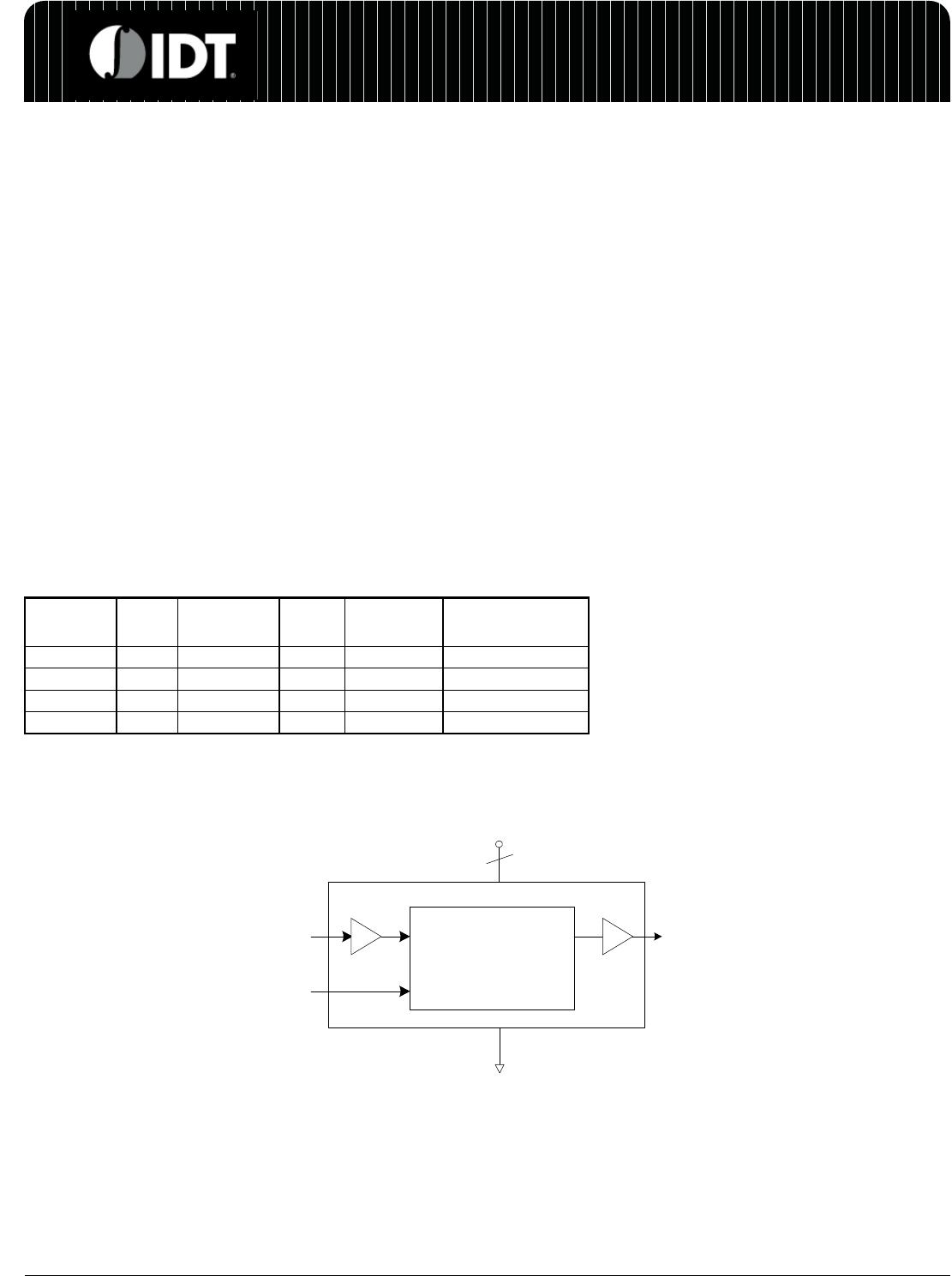
External Clock Input
This device operates from an external clock input and as
such does not have a on chip oscillator circuit.
PCB Layout Recommendations
For optimum device performance and lowest output phase
noise, the following guidelines should be observed.
1) The 0.01µF decoupling capacitors should be mounted on
the component side of the board as close to the VDD pin as
possible. No vias should be used between the decoupling
capacitors and VDD pins. The PCB trace to VDD pins
should be kept as short as possible, as should the PCB
trace to the ground via.
2) To minimize EMI, the 33Ω series termination resistor (if
needed) should be placed close to the clock output.
3) An optimum layout is one with all components on the
same side of the board, minimizing vias through other signal
layers. Other signal traces should be routed away from the
IDT5P50901/2/3/4. This includes signal traces just
underneath the device, or on layers adjacent to the ground
plane layer used by the device.
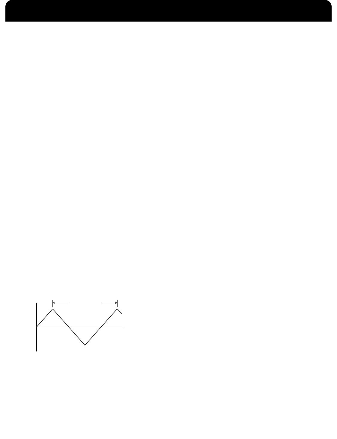
Spread Spectrum Profile
The IDT5P50901/2/3/4 is a low EMI clock generator using
an optimized frequency slew rate algorithm to facilitate down
stream tracking of zero delay buffers and other PLL devices.
The modulation rate is directly relate to the input clock
frequency.
For input frequency ICLK, then use the modulation
frequency indicated for the part below.
Time
Frequency
Modulation Rate

5P50903DVGI

Mfr. #:
Manufacturer:
IDT
Description:
Phase Locked Loops - PLL SPREAD SPECTRUM PLL
Lifecycle:
New from this manufacturer.
Delivery:
DHL FedEx Ups TNT EMS
Payment:
T/T Paypal Visa MoneyGram Western Union