_______________Detailed Description
The internal structures of the DG528/DG529 include
translators for the A2/A1/A0/EN/WR/RS digital inputs,
latches, and a decode section for channel selection
(Truth Tables). The gate structures consist of parallel
combinations of N and P MOSFETs.
WRITE (WR) and RESET (RS) strobes are provided for
interfacing with µP-bus lines (Figure 9), alleviating the
need for the µP to provide constant address inputs to
the mux to hold a particular channel.
When the WR strobe is in the low state (less than 0.8V)
and the RS strobe is in the high state (greater than
2.4V), the muxes are in the transparent mode—they act
similarly to nonlatching devices, such as the DG508A/
DG509A or the HI508/HI509.
When the WR goes high, the previous BCD address
input is latched and held in that state indefinitely. To
pull the mux out of this state, either WR must be taken
low to the transition state, or RS must be taken low to
turn off all channels.
RS turns off all channels when it is low, which resets
channel selection to the channel 1 mode.
The DG528/DG529 work with both single and dual sup-
plies and function over the +5V to +30V single-supply
range. For example, with a single +15V power supply,
analog signals in the 0V to +15V range can be
switched normally. If negative signals around 0V are
expected, a negative supply is needed. However, only
-5V is needed to normally switch signals in the -5V to
+15V range (-5V, +15V supplies). No current is drawn
from the negative supply, so Maxim’s MAX635 DC-DC
converter is an ideal choice.
The EN latch allows all switches to be turned off under
program control. This is useful when two or more
DG528s are cascaded to build 16-line and larger ana-
log-signal multiplexers.
DG528/DG529
8-Channel Latchable Multiplexers
_______________________________________________________________________________________ 7
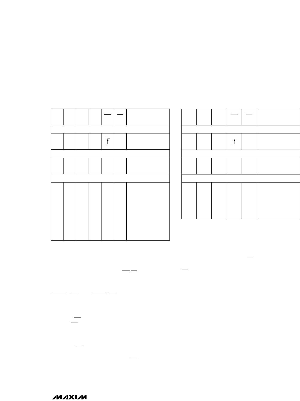
Table 1. DG528 Logic States Table 2. DG529 Logic States
A2 A1 A0 EN WR RS ON SWITCH
Latching
X X X X 1
Maintains previous
switch condition
Reset
X X X X X 0
None
(latches cleared)
Transparent Operation
X
0
0
0
0
1
1
1
1
X
0
0
1
1
0
0
1
1
X
0
1
0
1
0
1
0
1
0
1
1
1
1
1
1
1
1
0
0
0
0
0
0
0
0
0
1
1
1
1
1
1
1
1
1
None
1
2
3
4
5
6
7
8
A1 A0 EN WR RS ON SWITCH
X X X 1
Maintains previous
switch condition
X X X X 0
None
(latches cleared)
X
0
0
1
1
X
0
1
0
1
0
1
1
1
1
0
0
0
0
0
1
1
1
1
1
None
1
2
3
4
Latching
Reset
Transparent Operation
Note: Logic “1”: V
AH
2.4V, Logic “0”: V
AL
0.8V.
DG528/DG529
8-Channel Latchable Multiplexers
8 _______________________________________________________________________________________
PROTECTION
V-
Sn
S1
D
V+
CLK
RESET
4-WIDE LATCH
RS
PROTECTION
WR
PROTECTION
A_
PROTECTION
LEVEL SHIFT DECODE
EN
Figure 8. Simplified Internal Structure
_______________________Applications
Operation with Supply Voltages
Other Than ±15V
Maxim guarantees the DG528/DG529 for operation
from ±4.5V to ±20V supplies. The switching delays
increase by about a factor of two at ±5V, and break-
before-make action is preserved.
The DG528/DG529 can operate with a single +5V to
+30V supply as well as asymmetrical power supplies
like +15V and -5V. The digital threshold will remain
approximately 1.6V above the GND pin, and the analog
characteristics such as r
DS(ON)
are determined by the
total voltage difference between V+ and V-. Connect V-
to 0V when operating with a +5V to +30V single supply.
Digital Interface Levels
The typical digital threshold of both the address lines
and EN is 1.6V with a temperature coefficient of
approximately -3mV/°C, ensuring compatibility with TTL
logic over the temperature range. The digital threshold
is relatively independent of the power-supply voltages,
going from a typical 1.6V when V+ is 15V to 1.5V typi-
cal with V+ = 5V. Therefore, Maxim’s DG528/DG529
operate with standard TTL logic levels, even with ±5V
power supplies. In all cases, EN’s threshold is the same
as the other logic inputs and is referenced to GND.
The digital inputs can also be driven with CMOS logic
levels swinging from either V+ to V- or from V+ to GND.
The digital input current is just a few nanoamps of leak-
age at all input-voltage levels with a guaranteed maxi-
mum of 1µA. The digital inputs are protected from ESD
by a 30V zener diode between the input and V+ and
can be driven ±2V beyond the supplies without draw-
ing excessive current.
DG528/DG529
8-Channel Latchable Multiplexers
_______________________________________________________________________________________ 9
RESET
WR
CS
ADDRESS
BUS
±15V
ANALOG
INPUTS
1-OF-8
ANALOG
INPUTS
V+
+5V
-15V
+15V
V-
IN1
IN2
IN3
IN4
IN5
IN6
IN7
IN8
WR
RS
EN
A2
A1
A0
ADDRESS
DECODER
DATA BUS
MICROPROCESSOR
SYSTEM
BUS
7432
Figure 9. Bus Interface
18
17
16
15
14
13
12
11
1
2
3
4
5
6
7
8
RS
A1
GND
V+
S1B
S2B
S3B
S4B
DB
WR
A0
EN
V-
S1A
S2A
S3A
S4A
DA
TOP VIEW
10
9
DIP/SO
LCC/PLCC
DG529
14
15
16
17
184
5
6
7
8
3
2
1
20
19
9
10
11
12
13
DG528
EN
V
SS
S1
S2
S3
A2
GND
V
DD
S5
S6
A0
WR
N.C.
RS
A1
S4
D
N.C.
S8
S7
LCC/PLCC
14
15
16
17
184
5
6
7
8
3
2
1
20
19
9
10
11
12
13
DG529
EN
V
SS
S1A
S2A
S3A
GND
V
DD
S1B
S2B
S3B
A0
WR
N.C.
RS
A1
S4A
DA
N.C.
DB
S4B
N.C. = NO CONNECT
_____________________________________________Pin Configurations (continued)

DG529CWN+

Mfr. #:
Manufacturer:
Maxim Integrated
Description:
Multiplexer Switch ICs Dual 4:1 CMOS Mid V Latchable MUX
Lifecycle:
New from this manufacturer.
Delivery:
DHL FedEx Ups TNT EMS
Payment:
T/T Paypal Visa MoneyGram Western Union