NJM2748/2748A
- 4 -
Ver.2007-05-24
■IMPORTANT CONSIDERATIONS FOR USE OF NJM2748/2748A
•
••
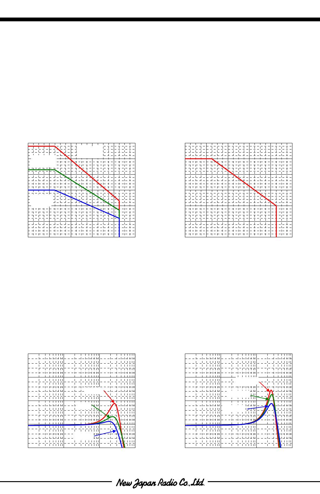
•Supply Current
When Ta25°C, Power Dissipation P
D
is limited by junction temperature (T
J
=125°C)
So maximum supply current is influenced by package, mounting board (board size, area of cupper foil), Mounting condition and
etc.
Following DMP8 Power Dissipation characteristic is a characteristic when mounted the following conditions supply.
• Two layer board: EIA/JEDEC 76.2×114.3×1.6mm, FR-4
• Four layer board: EIA/JEDEC 76.2×114.3×1.6mm, FR-4
Please refer to "Method of measuring the package thermal characteristic" published in our company web site for detailed
information on the thermal characteristic.
•
••
•THE OSCILLATION WITH A CAPACITIVE LOAD
NJM2748/2748A tends to oscillate easily when it uses voltage-follower, and driving capacitive load.
The figure below is a “Voltage Gain - Frequency characteristic” in the Voltage-Follower. (It is not the one to guarantee the
characteristic of the product.)
Especially, it becomes easy to oscillate in the condition that the input voltage (output voltage) is near the minus supply voltage
side and the condition with large output sink current. We will recommend use by some circuit gains.
Maximum Power Dissipation
−
−−
− Ambient Temperature
(DMP8)
0
100
200
300
400
500
600
0 20406080100
Ambient Temperature [ºC]
Power Dissipation P
D
[mW]
EIA/JEDEC
4-Layer
EIA/JEDEC
2-Layer
Package
Only
Maximum Power Dissipation
−
−−
− Ambient Temperature
(DIP8)
0
100
200
300
400
500
600
0 20406080100
Ambient Temperature [ºC]
Power Dissipation P
D
[mW]
Voltage Gain −
−−
− Frequency
(V
+
++
+
/V
−
−−
−
=±15V, Voltage Follower,
C
L
=100pF, I
SINK
=1mA, Ta=25ºC)
-5
0
5
10
15
10k 100k 1000k 10000k
Frequency [HZ]
Voltage Gain [dB]
V
O
=-10V
V
O
=0V
V
O
=+10V
1M 10M
Voltage Gain
−
−−
−
Frequency
(V
+
++
+
/V
−
−−
−
=±15V, Voltage Follower,
C
L
=100pF, V
O
=
−
−−
−
10V, Ta=25ºC)
-5
0
5
10
15
10k 100k 1000k 10000k
Frequency [HZ]
Voltage Gain [dB]
I
SINK
=5mA
I
SINK
=2mA
I
SINK
=1mA
1M 10M

