TC7USB42MU
4
10.
10.
10.
10. Electrical Characteristics
Electrical Characteristics
Electrical Characteristics
Electrical Characteristics
10.1.
10.1.
10.1.
10.1. DC Characteristics (Note) (Unless otherwise specified, T
DC Characteristics (Note) (Unless otherwise specified, T
DC Characteristics (Note) (Unless otherwise specified, T
DC Characteristics (Note) (Unless otherwise specified, T
a
a
a
a
= -40 to 85
= -40 to 85
= -40 to 85
= -40 to 85
)
)
)
)
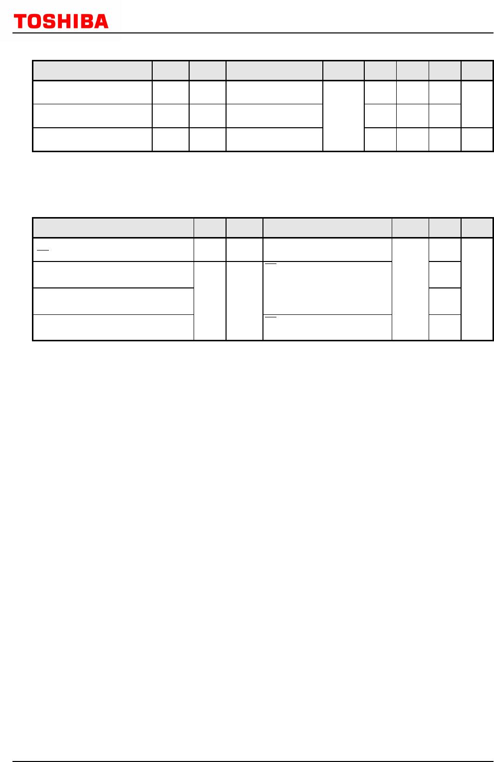
Characteristics
High-level input voltage (OE, S)
Low-level input voltage (OE, S)
Input leakage current (OE, S)
Power-OFF leakage current
Switch OFF-state leakage
current
ON-resistance
Difference of ON-resistance
between switches
ON-resistance flatness
Quiescent supply current
Symbol
V
IH
V
IL
I
IN
I
OFF
I
SZ
R
ON
∆R
ON
R
ON(flat)
I
CC
∆I
CC
Note
(Note 1)
(Note 1)
(Note 1)
Test Condition
V
IN
= 0 to 4.3 V
V
IN
= V
IS
= 0 to 4.3 V,
See Fig. 11.10
V
IS
= 0 to 3.6 V, OE = V
CC
,
See Fig. 11.11
V
IS
= 0 V, I
IS
= 30 mA,
See Fig. 11.9
V
IS
= 0.4 V, I
IS
= 30 mA,
See Fig. 11.9
V
IS
= 3.0 V, I
IS
= 30 mA,
See Fig. 11.9
V
IS
= 0.4 V, 1.0 V,
I
IS
= 30 mA
V
IS
= 0 V to 1.0 V,
I
IS
= 30 mA
V
IN
= V
CC
or GND,
I
OUT
= 0 A
V
IN
= 2.6 V (one input)
V
CC
(V)
2.3 to 3.0
3.0 to 4.3
2.3 to 4.3
2.3 to 4.3
0
2.3 to 4.3
3.0
3.0
3.0
3.0
3.0
4.3
4.3
Min
0.50 ×
V
CC
0.46 ×
V
CC
Typ.
4.5
4.8
10
0.35
1.3
Max
0.25 ×
V
CC
±1
±2
±2
6
6.7
14
1
40
Unit
V
µA
Ω
µA
Note: All typical values are at T
a
= 25.
Note 1: Measured by the voltage drop between D+/D- and 1D+/1D-,2D+/2D- pins at the indicated current through the
switch. On-resistance is determined by the lower of the voltages on the two pins.
10.2.
10.2.
10.2.
10.2. AC Characteristics (Note) (Unless otherwise specified, T
AC Characteristics (Note) (Unless otherwise specified, T
AC Characteristics (Note) (Unless otherwise specified, T
AC Characteristics (Note) (Unless otherwise specified, T
a
a
a
a
= -40 to 85
= -40 to 85
= -40 to 85
= -40 to 85
)
)
)
)
Characteristics
Propagation delay time
Turn-ON time
(S, OE to output)
Turn-OFF time
(S, OE to output)
Break before make
Skew of opposite transitions of
the same output (t
PHL
- t
PLH
)
Output skew (center port to any
other port)
Symbol
t
PLH
/
t
PHL
t
on
t
off
TBBM
t
SK(P)
t
SK(O)
Note
(Note 1)
(Note 1)
(Note 1)
Test Condition
C
L
= 5 pF, See Fig. 11.1
R
L
= 50 Ω, C
L
= 5 pF,
See Fig. 11.2
R
L
= 50 Ω, C
L
= 5 pF,
See Fig. 11.3
C
L
= 5 pF, See Fig. 11.4
C
L
= 5 pF, See Fig. 11.5
V
CC
(V)
3.3 ± 0.3
Min
2
Typ.
0.25
10
14
0.1
0.1
Max
20
24
7
Unit
ns
Note: All typical values are at T
a
= 25.
Note 1: Parameter guaranteed by design.
2013-02-05
Rev.2.0