ZLNB2015
ZLNB2015
Document number: DS32061 Rev. 1 - 2
5 of 7
www.diodes.com
January 2010
© Diodes Incorporated
NEW PRODUCT
Product Line o
Diodes Incorporated
Applications Information
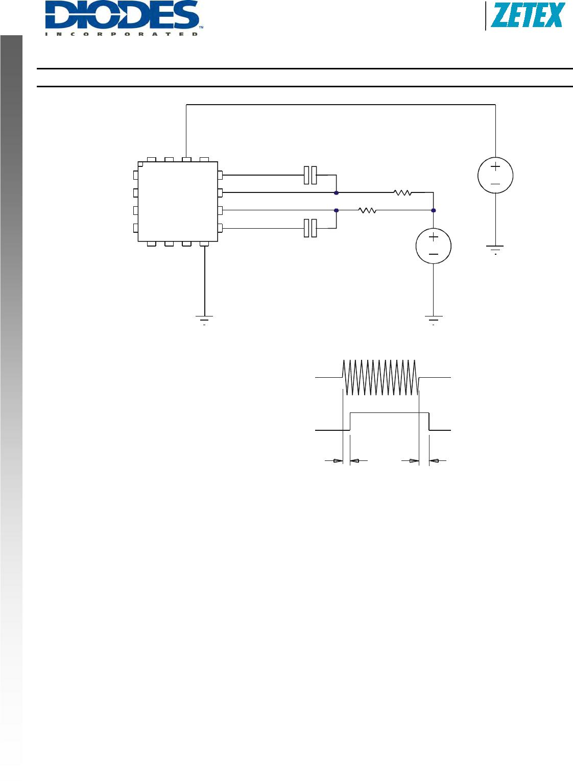
Above is a partial applications circuit for the ZLNB2015 showing all external components needed for a typical twin LNB design.
The inputs Vpol1 and Vpol2 are designed to be wired to the power inputs of the LNB via ESD protection resistors (6.8k). These
inputs control the HOR1/2, BHOR1/2 and ENA1/2 logic outputs. The HOR outputs will be low when their corresponding Vpol input
is at or below 14V and high when Vpol is at or above 14.5V. The BHOR outputs give inverted versions of their related HOR
outputs. The HOR/BHOR outputs are intended to activate polarisation selection circuitry within an LNB, under control of the LNB
supply voltage. The ENA1/2 outputs are set high when their corresponding Vpol input is at or above 8.5V and low when Vpol is at
or below 7.5V. These logic outputs can be used to disable any LNB RF output connected to a receiver (STB) that has been
powered down or disconnected (and hence not providing correct cable matching).
The ZLNB2015 includes circuitry necessary to detect the presence of a 22kHz tone modulated on either of two supply inputs to
the LNB. These detectors control the TD1/2 and BTD1/2 outputs. The TD outputs are set high on detection of a valid tone on their
corresponding LNB input and low in the absence of a tone. The BTD outputs give an inverted version of their corresponding TD
outputs. The main elements of each tone detector are an amplifier, a band-pass filter, a rectifier/smoother and a comparator. User
control is given over the gain of the amplifier and the lower frequency limit of the filter, using an external resistor and capacitor.
(The ESD protection resistor noted above can be used to set amplifier gain, hence requiring only one component for both
functions.) The higher frequency limit of the filter is set internally to block signals above 100kHz. The comparator circuit utilises no
external components.
The HOR, BHOR, TD, BTD and ENA outputs are designed to be compatible with LSTTL, CMOS and common MIMIC multiplexer
loads. Any input or output that is not required can be left open circuit.
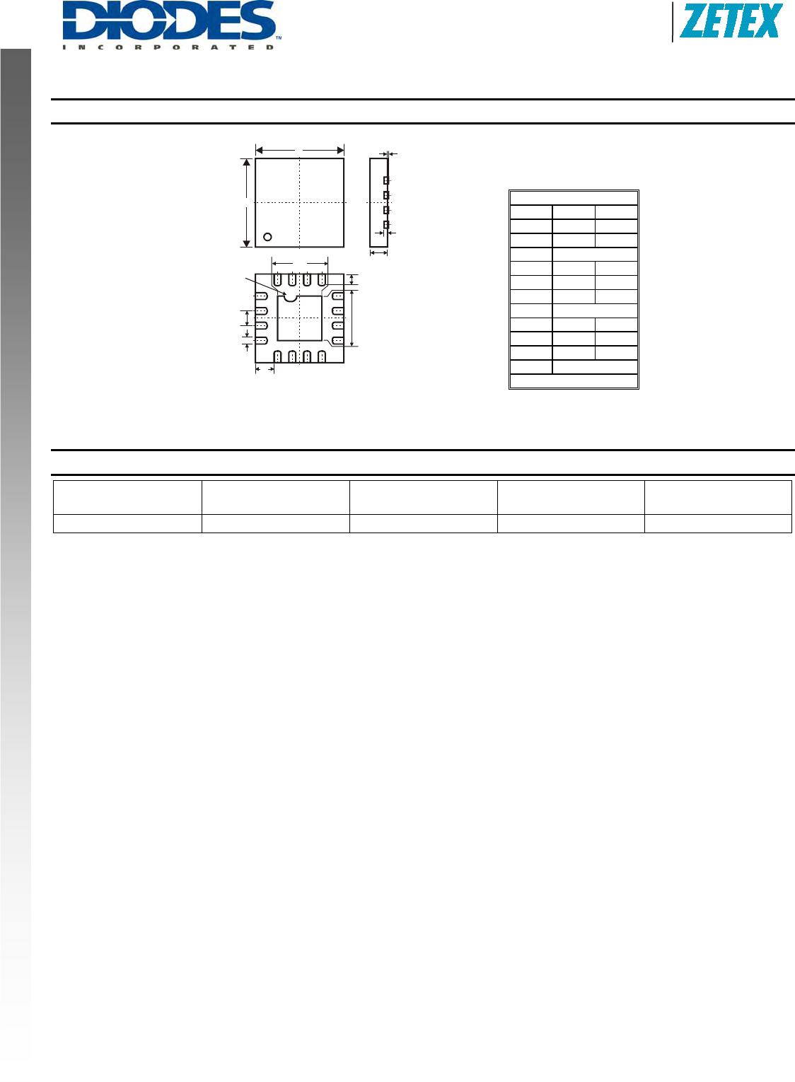
Output Truth Table
The ZLNB2015 includes two independent channels, each containing a voltage detector and tone detector. The following truth table
applies to each channel.
Tone Vpol TD BTD HOR BHOR ENA
Off 14V Low High Low High High
Off 14.5V Low High High Low High
On 14V High Low Low High High
On 14.5V High Low High Low High
- <7.5V - - Low High Low
C1
180pF
R1
6.8k
C2
180pF
ZLNB2015
R2
6.8k
BTD1
BHOR2
BTD2
TD2
HOR2
BHOR1
HOR1
VCC
ENA1
FIN1TD1
VPOL1
ENA2
GND
VPOL2
FIN2
Downfeed 1
Downfeed 2