VS-MURB820-M3, VS-MURB820-1-M3
www.vishay.com
Vishay Semiconductors
Revision: 25-Oct-17
4
Document Number: 96392
For technical questions within your region: DiodesAmericas@vishay.com
, DiodesAsia@vishay.com, DiodesEurope@vishay.com
THIS DOCUMENT IS SUBJECT TO CHANGE WITHOUT NOTICE. THE PRODUCTS DESCRIBED HEREIN AND THIS DOCUMENT
ARE SUBJECT TO SPECIFIC DISCLAIMERS, SET FORTH AT www.vishay.com/doc?91000
Fig. 7 - Typical Reverse Recovery Time vs. dI
F
/dt Fig. 8 - Typical Stored Charge vs. dI
F
/dt
Note
(1)
Formula used: T
C
= T
J
- (Pd + Pd
REV
) x R
thJC
;
Pd = forward power loss = I
F(AV)
x V
FM
at (I
F(AV)
/D) (see fig. 6);
Pd
REV
= inverse power loss = V
R1
x I
R
(1 - D); I
R
at V
R1
= rated V
R
Fig. 9 - Reverse Recovery Waveform and Definitions
100 1000
t
rr
(ns)
dI
F
/dt (A/µs)
20
40
V
R
= 160 V
T
J
= 125 °C
T
J
= 25 °C
30
50
10
I
F
= 16 A
I
F
= 8 A
I
F
= 4 A
100 1000
Q
rr
(nC)
dI
F
/dt (A/µs)
40
I
F
= 16 A
I
F
= 8 A
I
F
= 4 A
200
120
V
R
= 160 V
T
J
= 125 °C
T
J
= 25 °C
80
160
0
Q
rr
0.5 I
RRM
di
(rec)M
/dt
0.75 I
RRM
I
RRM
t
rr
t
b
t
a
I
F
di
F
/dt
0
(1)
(2)
(3)
(4)
(5)
(1) di
F
/dt - rate of change of current
through zero crossing
(2) I
RRM
- peak reverse recovery current
(3) t
rr
- reverse recovery time measured
from zero crossing point of negative
going I
F
to point where a line passing
through 0.75 I
RRM
and 0.50 I
RRM
extrapolated to zero current.
(4) Q
rr
- area under curve dened by t
rr
and I
RRM
t
rr
x I
RRM
2
Q
rr
=
(5) di
(rec)M
/dt - peak rate of change of
current during t
b
portion of t
rr
VS-MURB820-M3, VS-MURB820-1-M3
www.vishay.com
Vishay Semiconductors
Revision: 25-Oct-17
5
Document Number: 96392
For technical questions within your region: DiodesAmericas@vishay.com
, DiodesAsia@vishay.com, DiodesEurope@vishay.com
THIS DOCUMENT IS SUBJECT TO CHANGE WITHOUT NOTICE. THE PRODUCTS DESCRIBED HEREIN AND THIS DOCUMENT
ARE SUBJECT TO SPECIFIC DISCLAIMERS, SET FORTH AT www.vishay.com/doc?91000
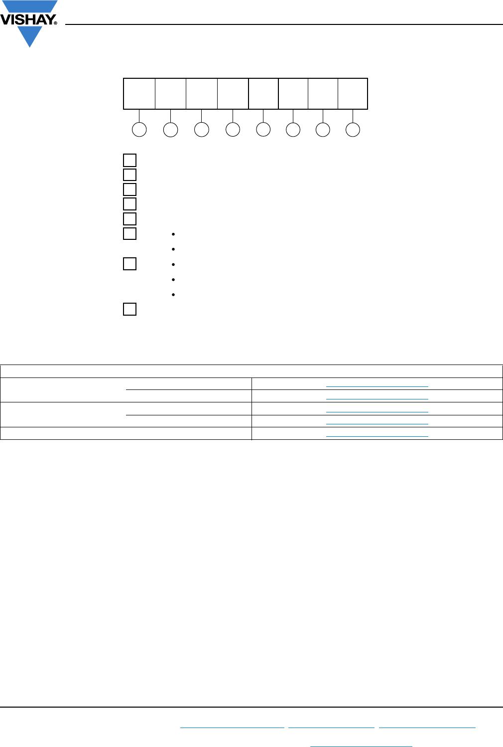
ORDERING INFORMATION TABLE
LINKS TO RELATED DOCUMENTS
Dimensions
D
2
PAK (TO-263AB) www.vishay.com/doc?96164
TO-262AA www.vishay.com/doc?96165
Part marking information
D
2
PAK (TO-263AB) www.vishay.com/doc?95444
TO-262AA www.vishay.com/doc?95443
Packaging information D
2
PAK (TO-263AB) www.vishay.com/doc?96424
Part Marking Information
www.vishay.com
Vishay Semiconductors
Revision: 21-Jun-17
1
Document Number: 95443
For technical questions within your region: DiodesAmericas@vishay.com
, DiodesAsia@vishay.com, DiodesEurope@vishay.com
THIS DOCUMENT IS SUBJECT TO CHANGE WITHOUT NOTICE. THE PRODUCTS DESCRIBED HEREIN AND THIS DOCUMENT
ARE SUBJECT TO SPECIFIC DISCLAIMERS, SET FORTH AT www.vishay.com/doc?91000
TO-262
Note
(1)
If part number contain “H” as last digit, product is AEC-Q101 qualified
ENVIRONMENTAL NAMING CODE (Z) PRODUCT DEFINITION
A Termination lead (Pb)-free
BTotally lead (Pb)-free
E RoHS-compliant and termination lead (Pb)-free
F RoHS-compliant and totally lead (Pb)-free
M Halogen-free, RoHS-compliant and termination lead (Pb)-free
N Halogen-free, RoHS-compliant and totally lead (Pb)-free
G Green
xxxxxxx-1
(1)
AC
Assembly
lot code
Part number
V ZYWWX
Product version (optional):
Z (replaced according below table)
Date code:
Year 1 = 2001
Week 19
Line X
Example: This is a xxxxxxx-1
(1)
with
assembly lot code AC,
assembled on WW 19, 2001
in the assembly line ”X”

VS-MURB820TRL-M3

Mfr. #:
Manufacturer:
Vishay Semiconductors
Description:
Rectifiers 200V 8A IF (TO-263AB) 100A IFSM
Lifecycle:
New from this manufacturer.
Delivery:
DHL FedEx Ups TNT EMS
Payment:
T/T Paypal Visa MoneyGram Western Union