LT6552
13
6552f
Layout and Passive Components
With a bandwidth of 75MHz and a slew rate of 600V/µs, the
LT6552 requires special attention to board layout and
supply bypassing. Use a ground plane, short lead lengths
and RF quality low ESR supply bypass capacitors. The
positive supply pin should be bypassed with a small
capacitor (typically 0.1µF) within 1 inch of the pin. When
driving loads greater than 10mA, an additional 4.7µF
electrolytic capacitor should be used. When using split
supplies, the same is true for the negative supply pin. The
parallel combination of the feedback resistor and gain
setting resistor on Pin 8 (FB) can combine with the input
capacitance to form a pole which can degrade stability. In
general, use feedback resistors of 1k or less.
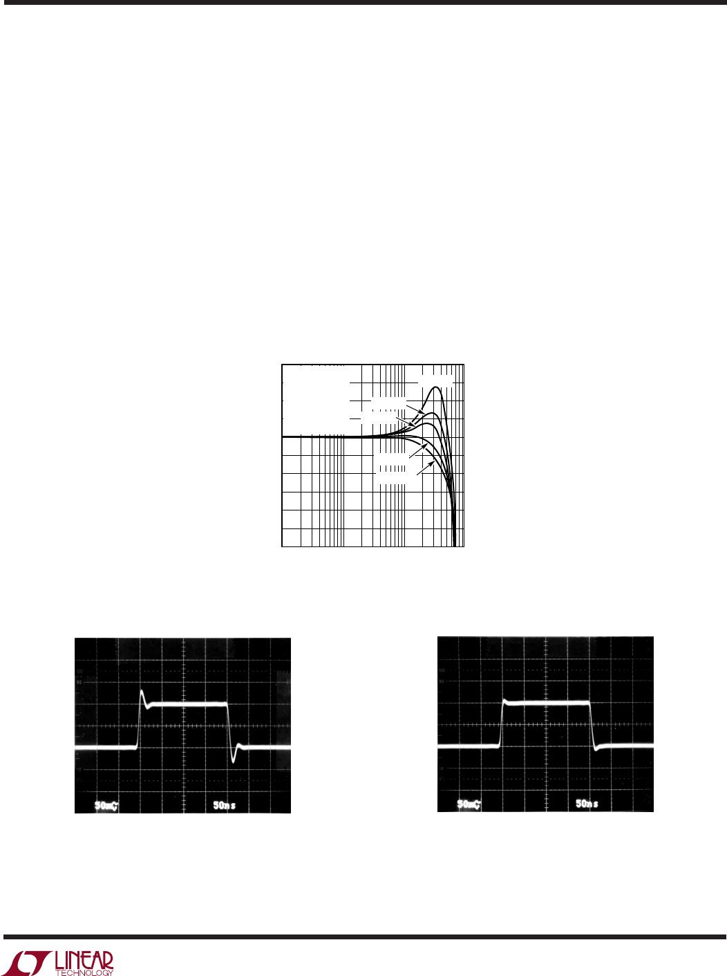
Operating with Low Closed-Loop Gains
The LT6552 has been optimized for closed-loop gains of
2 or greater. For a closed-loop gain of 2 the response
peaks about 3dB. Peaking can be reduced by using low
value feedback resistors, and can be eliminated by placing
a capacitor across the feedback resistor (feedback zero).
Figure 6 shows the closed-loop gain of 2 frequency
response with various values of the feedback capacitor.
This peaking shows up as a time domain overshoot of
40%; with an 8pF feedback capacitor the overshoot is
eliminated. Figures 7A and 7B show the Small Signal
Response of the LT6552 with and without an 8pF feedback
capacitor.
Figure 6. Closed-Loop Gain vs Frequency
Figure 7A. Small Signal Transient
Response, V
S
= 3.3V, 0V
Figure 7B. Small Signal Transient Response,
V
S
= 3.3V, 0V with 8pF Feedback Capacitor
FREQUENCY (MHz)
0.1
CLOSED-LOOP VOLTAGE GAIN (dB)
10
9
8
7
6
5
4
3
2
1
0
1 10 100
6552 F06
A
V
= 2
R
F
= R
G
= 500
R
L
= 150
T
A
= 25°C
V
OUT
= 1.5V DC
V
S
= 3.3V, 0V
C
F
= 0pF
C
F
= 3pF
C
F
= 5pF
C
F
= 8pF
C
F
= 10pF
APPLICATIO S I FOR ATIO
WUUU
1.5V
1.5V
A
V
= 2
R
F
= R
G
= 500
R
L
= 150
A
V
= 2
C
F
= 8pF
R
F
= R
G
= 500
R
L
= 150
50ns/DIV
50mV/DIV
50mV/DIV
50ns/DIV
6552 F07a
6552 F07b
LT6552
14
6552f
SHDN Pin
The LT6552 includes a shutdown feature that disables the
part, reducing quiescent current and making the output
high impedance. The part can be shutdown by bringing the
SHDN pin within 0.5V of V
. When shutdown the supply
current is typically 400µA and the output leakage current
DD Package
8-Lead Plastic DFN (3mm × 3mm)
(Reference LTC DWG # 05-08-1698)
is 0.25µA (V
V
OUT
V
+
). In normal operation the SHDN
can be tied to V
+
or left floating; if the pin is left uncon-
nected, an internal FET pull-up will keep the LT6552 fully
operational.
APPLICATIO S I FOR ATIO
WUUU
U
PACKAGE DESCRIPTIO
3.00 ±0.10
(4 SIDES)
NOTE:
1. DRAWING TO BE MADE A JEDEC PACKAGE OUTLINE M0-229 VARIATION OF (WEED-1)
2. DRAWING NOT TO SCALE
3. ALL DIMENSIONS ARE IN MILLIMETERS
4. DIMENSIONS OF EXPOSED PAD ON BOTTOM OF PACKAGE DO NOT INCLUDE
MOLD FLASH. MOLD FLASH, IF PRESENT, SHALL NOT EXCEED 0.15mm ON ANY SIDE
5. EXPOSED PAD SHALL BE SOLDER PLATED
6. SHADED AREA IS ONLY A REFERENCE FOR PIN 1 LOCATION
ON TOP AND BOTTOM OF PACKAGE
0.38 ± 0.10
BOTTOM VIEW—EXPOSED PAD
1.65 ± 0.10
(2 SIDES)
0.75 ±0.05
R = 0.115
TYP
2.38 ±0.10
(2 SIDES)
14
85
PIN 1
TOP MARK
(NOTE 6)
0.200 REF
0.00 – 0.05
(DD8) DFN 1203
0.25 ± 0.05
2.38 ±0.05
(2 SIDES)
RECOMMENDED SOLDER PAD PITCH AND DIMENSIONS
1.65 ±0.05
(2 SIDES)2.15 ±0.05
0.50
BSC
0.675 ±0.05
3.5 ±0.05
PACKAGE
OUTLINE
0.25 ± 0.05
0.50 BSC
LT6552
15
6552f
PACKAGE DESCRIPTIO
U
.016 – .050
(0.406 – 1.270)
.010 – .020
(0.254 – 0.508)
× 45°
0°– 8° TYP
.008 – .010
(0.203 – 0.254)
SO8 0303
.053 – .069
(1.346 – 1.752)
.014 – .019
(0.355 – 0.483)
TYP
.004 – .010
(0.101 – 0.254)
.050
(1.270)
BSC
1
2
3
4
.150 – .157
(3.810 – 3.988)
NOTE 3
8
7
6
5
.189 – .197
(4.801 – 5.004)
NOTE 3
.228 – .244
(5.791 – 6.197)
.245
MIN
.160
±.005
RECOMMENDED SOLDER PAD LAYOUT
.045 ±.005
.050 BSC
.030 ±.005
TYP
INCHES
(MILLIMETERS)
NOTE:
1. DIMENSIONS IN
2. DRAWING NOT TO SCALE
3. THESE DIMENSIONS DO NOT INCLUDE MOLD FLASH OR PROTRUSIONS.
MOLD FLASH OR PROTRUSIONS SHALL NOT EXCEED .006" (0.15mm)
S8 Package
8-Lead Plastic Small Outline (Narrow .150 Inch)
(Reference LTC DWG # 05-08-1610)
Information furnished by Linear Technology Corporation is believed to be accurate and reliable.
However, no responsibility is assumed for its use. Linear Technology Corporation makes no represen-
tation that the interconnection of its circuits as described herein will not infringe on existing patent rights.

LT6552IDD#PBF

Mfr. #:
Manufacturer:
Analog Devices Inc.
Description:
Video Amplifiers 3.3V Single Supply Video Difference Amp
Lifecycle:
New from this manufacturer.
Delivery:
DHL FedEx Ups TNT EMS
Payment:
T/T Paypal Visa MoneyGram Western Union