NCN8025 / NCN8025A
www.onsemi.com
4
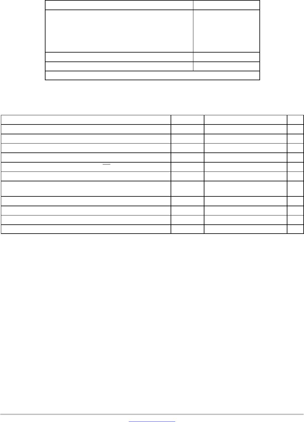
PIN FUNCTION AND DESCRIPTION
Pin
(QFN24)
DescriptionTypeName
Pin
(QFN16)
6 − CAUX2 Input/
Output
This pin handles the connection to the chip card’s serial auxiliary AUX2 I/O pin (C8). A
bi−directional level translator adapts the serial I/O signal between the card and the micro
controller. A 11 kW (typical) pull up resistor to CVCC provides a High impedance state for
the smart card C8 pin.
7 − CAUX1 Input/
Output
This pin handles the connection to the chip card’s serial auxiliary AUX1 I/O pin (C4). A
bi−directional level translator adapts the serial I/O signal between the card and the micro
controller. A 11 kW (typical) pull up resistor to CVCC provides a High impedance state for
the smart card C4 pin.
8 − GND Ground Card Ground
9 5 CCLK Output This pin is connected to the CLOCK card connector’s pin (Chip card’s pin C3). The Clock
signal comes from the CLKIN input through clock dividers and level shifter.
10 6 CRST Output This pin is connected to the chip card’s RESET pin (C2) through the card connector. A
level translator adapts the external Reset (RSTIN) signal to the smart card.
11 7 CVCC Power
Output
This pin is connected to the smart card power supply pin (C1). An internal low dropout
regulator is programmable using the pins VSEL0 and VSEL1 to supply either 5 V or 3 V
or 1.8 V output voltage. An external distributed ceramic capacitor ranging from 80 nF to
1.2 mF recommended must be connected across CVCC and CGND. This set of capacitor
(if distributed) must be low ESR (< 100 mW).
12 8 CMDVCC Input Command V
CC
pin. Activation sequence Enable/Disable pin (active Low). The activation
sequence is enabled by toggling CMDVCC
High to Low and when a card is present.
13 − PORADJ Input Power−on reset threshold adjustment input pin for changing the reset threshold (V
DD
UVLO threshold) thanks to an external resistor power divider. Needs to be connected to
ground when unused.
14 9 RSTIN Input This Reset input connected to the host and referred to VDD (microcontroller side), is
connected to the smart card Reset pin through the internal level shifter which translates
the level according to the CVCC programmed value.
15 10 VDD Power
input
This pin is connected to the system controller power supply. It configures the level shifter
input stage to accept the signals coming from the controller. A 0.1 mF decoupling
capacitor shall be used. When V
DD
is below 2.30 V typical the card pins are disabled.
16 − GND Ground Ground
17 11 INT Output The interrupt request is activated LOW on this pin. This is enabled when a card is present
and the card presence is detected by PRES
or PRES pins. Similarly an interrupt is
generated when CVCC is overloaded. Inverter output (An open−drain output configuration
with 50 kW pull−up resistor is available under request (metal change)).
18 12 CLKIN Input Clock Input for External Clock
19 13 I/Ouc Input /
Output
This pin is connected to an external micro−controller. A bi−directional level translator
adapts the serial I/O signal between the smart card and the external controller. A built−in
constant 11 kW (typical) resistor provides a high impedance state.
20 − AUX1uc Input /
Output
This pin is connected to an external micro−controller. A bi−directional level translator
adapts the serial C4 signal between the smart card and the external controller. A built−in
constant 11 kW (typical) resistor provides a high impedance state.
21 − AUX2uc Input /
Output
This pin is connected to an external micro−controller. A bi−directional level translator
adapts the serial C8 signal between the smart card and the external controller. A built−in
constant 11 kW (typical) resistor provides a high impedance state.
22 14 CLKDIV1 Input This pin coupled with CLKDIV2 is used to program the clock frequency division ratio
(Table 2).
23 15 CLKDIV2 Input This pin coupled with CLKDIV1 is used to program the clock frequency division ratio
(Table 2).
24 16 VSEL1 Input Allows selecting card V
CC
power supply voltage.
VSEL0 = Low: CVCC = 5 V when VSEL1 = High or 3 V when VSEL1 = Low.
VSEL0 = High: CVCC = 1.8 V when VSEL1 = High or 3 V when VSEL1 = Low.
25 17 GND Ground Regulator Power Supply Ground
NOTE: All information below refers to QFN−24 pin numbering unless otherwise noted. This information can be transposed to
the QFN−16 package according to the above “PIN FUNCTION AND DESCRIPTION” Table.