cui.com
CUI Inc │ SERIES: PRMC3-S │ DESCRIPTION: DC-DC CONVERTER date 05/05/2014 │ page 5 of 6
1. Output load requirement
To ensure this module can operate efciently and reliably, the minimum output load may not be less than 5% of the full load during
operation. If the actual output power is low, connect a resistor at the output end in parallel to increase the load.
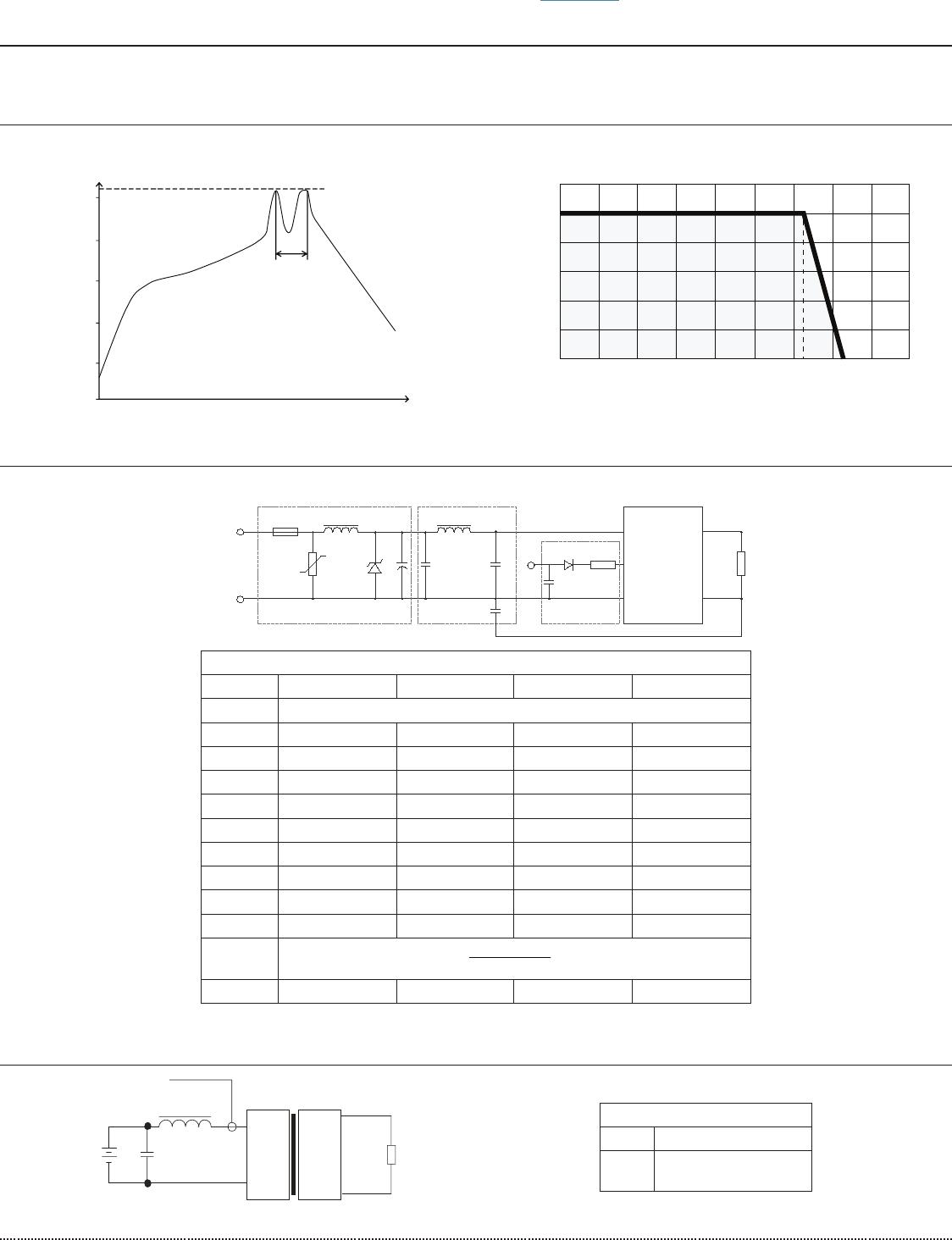
2. Recommended circuit
This series has been tested according to the following recommended testing circuit before leaving the factory. This series should
be tested under load (see Figure 3 and Table 3). If you want to further decrease the input/output ripple, you can increase the
capacitance accordingly or choose capacitors with low ESR. However, the capacitance of the output lter capacitor must be
appropriate. If the capacitance is too high, a startup problem might arise. For every channel of the output, to ensure safe and reliable
operation, the maximum capacitance must be less than the maximum capacitive load (see Table 4).
3. CTRL Terminal
When open or applied high impedance, the converter will turn on. When it’s pulled high, the converter will shutdown. The input
current should between 5~10mA. Exceeding the maximum 20mA will cause permanent damage to the converter. The value for R can
be derived as follows:
4. Input Current
When it is used in an unregulated condition, make sure that the input uctuations and ripple voltage do not exceed the module
standard. Refer to Figure 5 and Table 5 for the startup current of this dc-dc module.
Single
Vout
(Vdc)
Max. Capacitive
Load
(μF)
Dual
Vout
(Vdc)
Max. Capacitive
Load
1
(μF)
3.3 2700 -- --
5 2200 5 1000
9 1000 -- --
12 680 12 470
15 470 15 330
24 330 -- --
Table 4
Note: 1. For each output.
APPLICATION NOTES
Figure 3
Figure 5
Table 3
Vin
(Vdc)
Cin1
(µF)
Cin2
(µF)
Lin
(µH)
Cs
1
(µF)
Cout
(µF)
Lout
2
(µH)
Cd
(nF/V)
5 100 47 4.7~12 10~22 100 2.2~10 47/100
12 100 47 4.7~12 10~22 100 2.2~10 47/100
24 10 1 4.7~12 10~22 100 2.2~10 47/100
48 10 1 4.7~12 10~22 100 2.2~10 47/100
Single output Dual output
9R
9
&RXW
&V
&LQ
9LQ
*1'
9F
5
/LQ
,F
'
&G
&LQ
9R
9
&RXW
&RXW
/RXW
/RXW
9R
&LQ
9LQ
*1'
/LQ
9F
5
,F
'
&G
&LQ
Note: 1. For single output only
2. For dual output only
−
=
DC
I
Note: 1. Minimum load shouldn't be less than 5%, otherwise ripple may increase dramatically. Operation under minimum load will not damage the converter, however, they may
not meet all specications listed.
2. Maximum capacitive load is tested at input voltage range and full load.
3. All specications are measured at Ta=25°C, humidity<75%, nominal input voltage and rated output load unless otherwise specied.
Range
InputVoltage
Input Curre nt(A)
InputVoltage (V)
Ip
Vin
(Vdc)
Ip
(mA)
5 1110
12 640
24 325
48 160
Table 5
V
c
: Control pin input voltage
V
D
: Forward voltage drop of diode D1
I
C
: Input current to control pin
R: Resistor of control circuit
Vin
GND
+Vo
-Vo
(0V)
EUT
LOAD
Ctrl
Cd
D1
R
Vc
Figure 4
For more information, please visit the product page.