5
LTC1446/LTC1446L
1446L G13
TIME (10µs/DIV)
V
OUT
(2V/DIV)
CS/LD
(5V/DIV)
TYPICAL PERFORMANCE CHARACTERISTICS
U
W
LTC1446L Supply Current vs Logic
Input Voltage
LOGIC INPUT VOLTAGE (V)
0.5
1.0
1.1
1.2
1446/46L G10
0.9
0.8
1.0 1.5 2.0 2.5 3.0
0.7
0.6
0.5
SUPPLY CURRENT (mA)
LTC1446 Supply Current vs
Temperature
TEMPERATURE (°C)
–55
SUPPLY CURRENT (µA)
660
670
680
105
1446/46L G12
650
640
620
–15
25
65
–35 125
5
45
85
630
700
690
V
CC
= 3.3V
V
CC
= 2.7V
V
CC
= 3V
LTC1446L Supply Current
vs Temperature
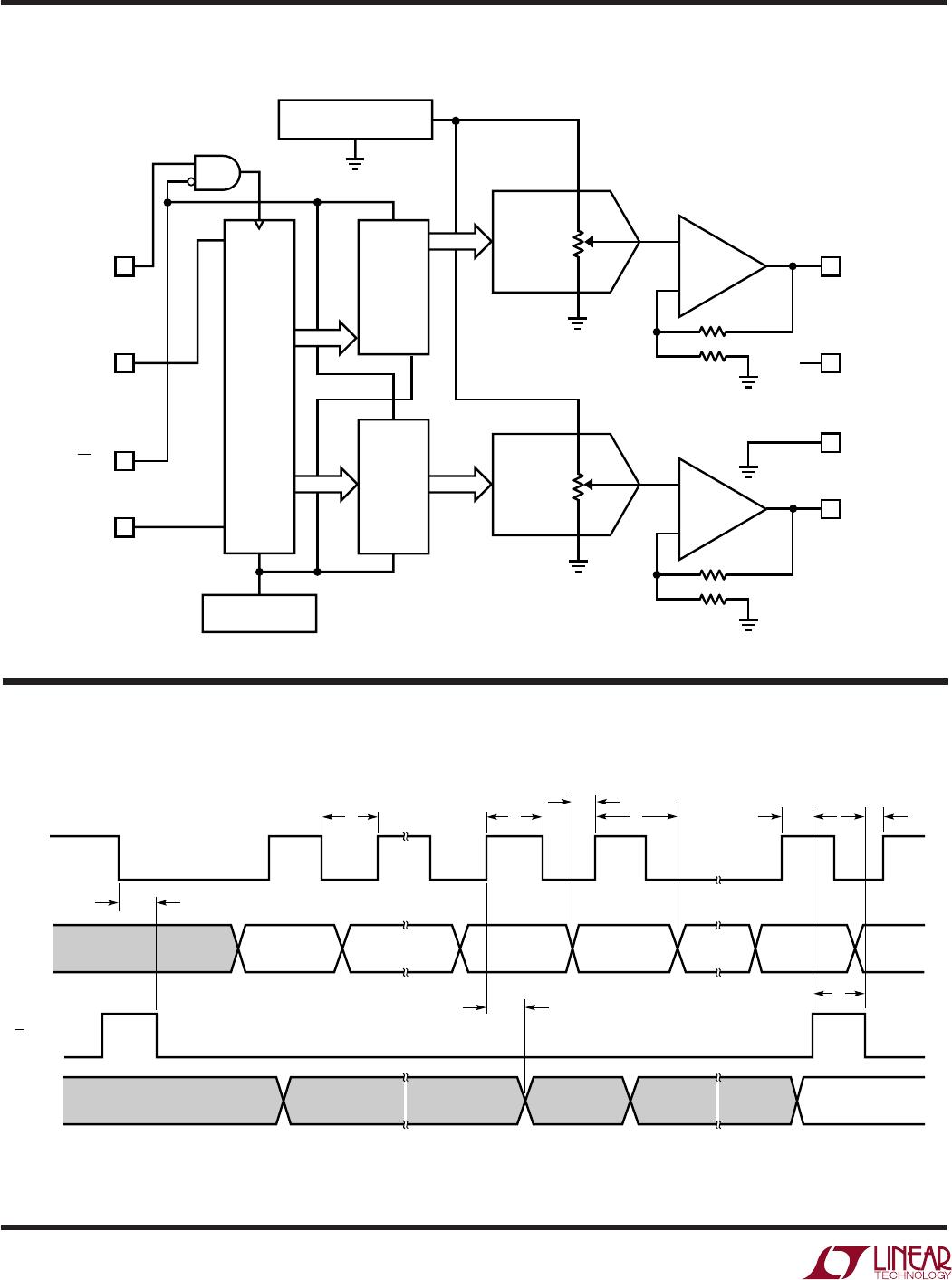
PIN FUNCTIONS
UUU
CLK: The Serial Interface Clock.
D
IN
: The Serial Interface Data.
CS/LD: The Serial Interface Enable and Load Control.
When CS/LD is low the CLK signal is enabled, so the data
can be clocked in. When CS/LD is pulled high data is
loaded from the shift register into the DAC registers,
updating the DAC outputs.
D
OUT
: The output of the shift register which becomes valid
on the rising edge of the serial clock.
GND: Ground.
V
OUT A
,V
OUT B
: Buffered DAC Outputs.
V
CC
: Positive Supply Input.
4.5V ≤ V
CC
≤ 5.5V (LTC1446), 2.7V ≤ V
CC
≤ 5.5V
(LTC1446L). Requires a 0.1µF bypass capacitor to
ground.
TEMPERATURE (°C)
–55 –35 –15 5 25 45 65 85 105
900
SUPPLY CURRENT (µA)
910
930
940
970
1446/46L G11
920
125
950
960
V
CC
= 5.5V
V
CC
= 4.5V
V
CC
= 5V
Large Signal Transient Response