LTC1041CN8#PBF

LTC1041
4
1041fa
APPLICATIO S I FOR ATIO
WUUU
The LTC1041 uses sampled data techniques to achieve
its unique characteristics. It consists of two comparators,
each of which has two differential inputs (Figure 1a).
When the sum of the voltages on a comparator’s inputs is
positive, the output is high and when the sum is negative,
the output is low. The inputs are interconnected such that
the R
S
flip-flop is reset (ON/OFF = GND) when
V
IN
> (SET POINT + DELTA) and is set (ON/OFF = V
+
) when
V
IN
< (SET POINT – DELTA). This makes a very precise
hysteresis loop of 2 • DELTA centered around the
SET POINT. (See Figure 1b.)
For R
S
< 10k
The dual differential input structure is made with CMOS
switches and a precision capacitor array. Input
impedance characteristics of the LTC1041 can be
determined from the equivalent circuit shown in Figure 2.
The input capacitance will charge with a time constant of
V
P-P
Output Voltage
vs Load Current
R
IN
vs Sampling Frequency
LOAD CURRENT, I
L
(mA)
0
TYPICAL OUTPUT VOLTAGE DROP (V
+
– V
P-P
)
(V)
0.8
0.4
0
8
LTC1041 • TPC06
1.2
1.6
2.0
0.6
0.2
1.0
1.4
1.8
21
43
67 9
5
10
V
+
= 2.8V
V
+
= 16V
V
+
= 5V
V
+
= 10V
SAMPLING FREQUENCY f
S
(Hz)
1
10
7
AVERAGE INPUT RESISTANCE, R
IN
(1/f
S
• 66pF) ()
10
9
10
11
10
2
10
4
10
3
10
LTC1041 • TPC07
10
8
10
10
TYPICAL PERFOR A CE CHARACTERISTICS
UW
LTC1041 • AI01a
OSC
(6)
GND
(4)
DELTA
(5)
SET POINT
(3)
V
IN
(2)
C
EXT
R
EXT
POWER ON
V
P-P
(7)
V
+
(8)
ON/OFF
(1)
V
+
V
+
80µs
4
+
+
COMP B
4
TIMING
GENERATOR
V
P-P
CIRCUIT
+
+
COMP A
(a)
LTC1041 • AI01b
V
+
GND
0V
INPUT VOLTAGE, V
IN
V
L
V
U
SET POINT
DEADBAND
DELTA –
+
DELTA
ON/OFF OUTPUT
Figure 1. LTC1041 Block Diagram
(b)
LTC1041
5
1041fa
APPLICATIO S I FOR ATIO
WUUU
R
S
• C
IN
. The ability to fully charge C
IN
from the signal
source during the controller’s active time is critical in
determining errors caused by the input charging current.
For source resistances less than 10k, C
IN
fully charges
and no error is caused by the charging current.
For R
S
> 10k
For source resistances greater than 10k, C
IN
cannot fully
charge, causing voltage errors. To minimize these errors,
an input bypass capacitor, C
S
, should be used. Charge is
shared between C
IN
and C
S
, causing a small voltage error.
The magnitude of this error is A
V
= V
IN
• C
IN
(C
IN
+ C
S
). This
error can be made arbitrarily small by increasing C
S
.
The averaging effect of the bypass capacitor, C
S
, causes
another error term. Each time the input switches cycle
between the plus and minus inputs, C
IN
is charged and
discharged. The average input current due to this is
I
AVG
= V
IN
• C
IN
• f
S
, where f
S
is the sampling frequency.
Because the input current is directly proportional to the
differential input voltage, the LTC1041 can be said to have
an average input resistance of R
IN
= V
IN
/I
AVG
= I/(f
S
• C
IN
).
Since two comparator inputs are connected in parallel, R
IN
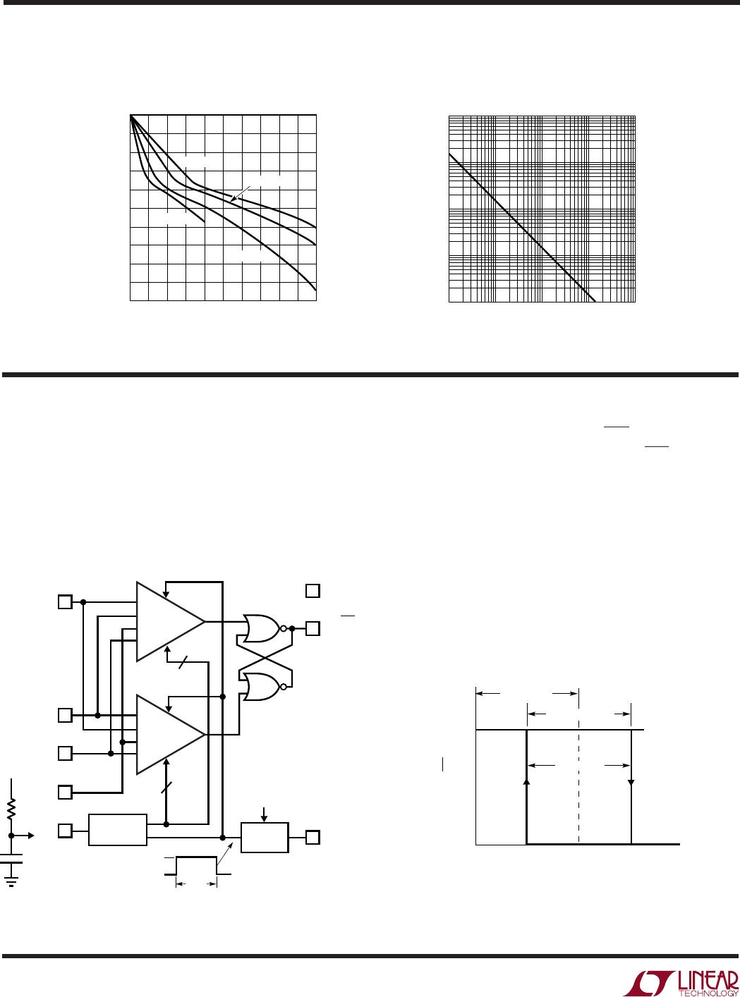
is one half of this value (see typical curve of R
IN
versus
Sampling Frequency). This finite input resistance causes
an error due to the voltage divider between R
S
and R
IN
.
The input voltage error caused by both of these effects is
V
ERROR
= V
IN
[2C
IN
/(2C
IN
+ C
S
) + R
S
/(R
S
+ R
IN
)].
Example: assume f
S
= 10Hz, R
S
= 1M, C
S
= 1µF, V
IN
= 1V,
V
ERROR
= 1V(66µV + 660µV) = 726µV. Notice that most of
the error is caused by R
IN
. If the sampling frequency is
reduced to 1Hz, the voltage error from the input
impedance effects is reduced to 136µV.
Figure 2. Equivalent Input Circuit
V
IN
R
S
C
S
LTC1041 • AI01
S1
S2
C
IN
( 33pF)
V
LTC1041 DIFFERENTIAL INPUT
+
Input Voltage Range
The input switches of the LTC1041 are capable of
switching either to the V
+
supply or ground. Consequently,
the input voltage range includes both supply rails. This is
a further benefit of the sampling input structure.
Error Specifications
The only measurable errors on the LTC1041 are the
deviations from “ideal” of the upper and lower switching
levels (Figure 1b). From a control standpoint, the error in
the SET POINT and deadband is critical. These errors may
be defined in terms of V
U
and V
L
.
SET POINT error
V
SET POINT
deadband error V
U
U
+
()
V
V DELTA
L
L
2
2
––
The specified error limits (see electrical characteristics)
include error due to offset, power supply variation, gain,
time and temperature.
Pulsed Power (V
P-P
) Output
It is often desirable to use the LTC1041 with resistive
networks such as bridges and voltage dividers. The power
consumed by these resistive networks can far exceed that
of the LTC1041 itself.
At low sample rates the LTC1041 spends most of its time
off. A switched power output, V
P-P
, is provided to drive the
input network, reducing its average power as well. V
P-P
is
switched to V
+
during the controller’s active time ( 80µs)
and to a high impedance (open circuit) when internal
power is switched off.
Figure 3 shows the V
P-P
output circuit. The V
P-P
output
voltage is not precisely controlled when driving a load
(see typical curve of V
P-P
Output Voltage vs Load Current).
In spite of this, high precision can be achieved in two ways:
(1) driving ratiometric networks and (2) driving fast set-
tling references.
In ratiometric networks all the inputs are proportional to
V
P-P
(Figure 4). Consequently, the absolute value of V
P-P
does not affect accuracy.
LTC1041
6
1041fa
APPLICATIO S I FOR ATIO
WUUU
If the best possible performance is needed, the inputs to
the LTC1041 must completely settle within 4µs of the start
of the comparison cycle (V
P-P
high impedance to V
+
transition). Also, it is critical that the input voltages do not
change during the 80µs active time. When driving resistive
input networks with V
P-P
, capacitive loading should be
minimized to meet the 4µs settling time requirement.
Further, care should be exercised in layout when driving
networks with source impedances, as seen by the LTC1041,
of greater than 10k (see For R
S
> 10k).
Figure 5. Driving Reference with V
P-P
Output
V
IN
I
L
LTC1041 • AI05
LT1009-2.5
8
7
6
5
1
2
3
4
LTC1041
SET POINT
DELTA
R2
R3
R4
R1
V
+
Figure 3. V
P-P
Output Switch
LTC1041 • AI03
80µs
COMPARATOR ON TIME
8
V
+
47
GND
Q1 P1
V
P-P
Figure 4. Ratiometric Network Driven by V
P-P
R3
R1
SET POINT
GND DELTA
V
IN
V
+
V
P-P
R2
R4
R5
R6
LTC1041 • AI04
8
7
6
5
1
2
3
4
LTC1041
In applications where an absolute reference is required,
the V
P-P
output can be used to drive a fast settling
reference. The LTC1009 2.5V reference settles in 2µs
and is ideal for this application (Figure 5). The current
through R1 must be large enough to supply the LT1009
minimum bias current ( 1mA) and the load current, I
L
.
Internal Oscillator
An internal oscillator allows the LTC1041 to strobe itself.
The frequency of the oscillation, and hence the sampling
rate, is set with an external RC network (see typical curve,
Sampling Rate R
EXT
, C
EXT
). R
EXT
and C
EXT
are connected
as shown in Figure 1. To assure oscillation, R
EXT
must be
between 100k and 10M. There is no limit to the size of
C
EXT
.
At low sampling rates, R
EXT
is very important in
determining the power consumption. R
EXT
consumes
power continuously. The average voltage at the OSC pin
is approximately V
+
/2, giving a power dissipation of
P
REXT
= (V
+
/ 2)
2
/R
EXT
.
Example: assume R
EXT
= 1M, V
+
= 5V, P
REXT
=
(2.5)
2
/10
6
= 6.25/µW. This is approximately four times the
power consumed by the LTC1041 at V
+
= 5V and
f
S
= 1 sample/second. Where power is a premium,
R
EXT
should be made as large as possible. Note that the
power dissipated by R
EXT
is
not
a function of f
S
or C
EXT
.
If high sampling rates are needed and power consumption
is of secondary importance, a convenient way to get the
maximum possible sampling rate is to make R
EXT
= 100k
and C
EXT
= 0. The sampling rate, set by the controller’s
active time, will nominally be 10kHz.
To synchronize the Sampling of the LTC1041 to an
external frequency source, the OSC pin can be driven by a
CMOS gate. A CMOS gate is necessary because the input
trip points of the oscillator are close to the supply rails and
TTL does not have enough output swing. Externally driven,
there will be a delay from the rising edge of the OSC input
and the start of the sampling cycle of approximately 5µs.

LTC1041CN8#PBF

Mfr. #:
Manufacturer:
Analog Devices Inc.
Description:
Analog Comparators Bang-Bang Controller
Lifecycle:
New from this manufacturer.
Delivery:
DHL FedEx Ups TNT EMS
Payment:
T/T Paypal Visa MoneyGram Western Union

Products related to this Datasheet