4
FN6048.10
September 3, 2015
Absolute Maximum Ratings Thermal Information
V
CC
to Ground. . . . . . . . . . . . . . . . . . . . . . . . . . . . . . . . . . . . . . . 7V
Input Voltages
DI, DE, RE
. . . . . . . . . . . . . . . . . . . . . . . . . . -0.5V to (V
CC
+0.5V)
Input/Output Voltages
A/Y, B/Z . . . . . . . . . . . . . . . . . . . . . . . . . . . . . . . . . -8V to +12.5V
RO . . . . . . . . . . . . . . . . . . . . . . . . . . . . . . . . -0.5V to (V
CC
+0.5V)
Short Circuit Duration
Y, Z . . . . . . . . . . . . . . . . . . . . . . . . . . . . . . . . . . . . . . . Continuous
ESD Rating . . . . . . . . . . . . . . . . . . . . . . . . . See Specification Table
Operating Conditions
Temperature Range
ISL8485ECx . . . . . . . . . . . . . . . . . . . . . . . . . . . . . . . 0°C to +70°C
ISL848xEIx. . . . . . . . . . . . . . . . . . . . . . . . . . . . . . -40°C to +85°C
ISL8485EAx . . . . . . . . . . . . . . . . . . . . . . . . . . . . -40°C to +125°C
ISL8485EMx. . . . . . . . . . . . . . . . . . . . . . . . . . . . -55°C to +125°C
Thermal Resistance (Typical, Note 1)
JA
(°C/W)
8 Ld SOIC Package . . . . . . . . . . . . . . . . . . . . . . . . . 170
8 Ld PDIP Package* . . . . . . . . . . . . . . . . . . . . . . . . 140
Maximum Junction Temperature (Plastic Package) . . . . . . +150°C
Maximum Storage Temperature Range . . . . . . . . . . -65°C to +150°C
Pb-free reflow profile . . . . . . . . . . . . . . . . . . . . . . . . . .see link below
http://www.intersil.com/pbfree/Pb-FreeReflow.asp
*Pb-free PDIPs can be used for through hole wave solder processing
only. They are not intended for use in reflow solder processing
applications.
CAUTION: Do not operate at or near the maximum ratings listed for extended periods of time. Exposure to such conditions may adversely impact product reliability and
result in failures not covered by warranty.
NOTE:
1.
JA
is measured with the component mounted on a low effective thermal conductivity test board in free air. See Tech Brief TB379 for details.
Electrical Specifications Test Conditions: V
CC
= 4.5V to 5.5V; Unless Otherwise Specified.
Typicals are at V
CC
= 5V, T
A
= +25°C, (Note 2)
PARAMETER SYMBOL TEST CONDITIONS
TEMP
(°C)
MIN
(Note 12) TYP
MAX
(Note 12) UNITS
DC CHARACTERISTICS
Driver Differential V
OUT
(no load) V
OD1
Full - - V
CC
V
Driver Differential V
OUT
(with load) V
OD2
R = 50 (RS-422), (Figure1) Full 2 3 - V
R = 27 (RS-485), (Figure 1) Full 1.5 2.3 5 V
Change in Magnitude of Driver
Differential V
OUT
for
Complementary Output States
V
OD
R = 27 or 50, (Figure 1) Full - 0.01 0.2 V
Driver Common-Mode V
OUT
V
OC
R = 27 or 50, (Figure 1) Full - - 3 V
Change in Magnitude of Driver
Common-Mode V
OUT
for
Complementary Output States
V
OC
R = 27 or 50, (Figure 1) Full - 0.01 0.2 V
Logic Input High Voltage V
IH
DE, DI, RE Full 2 - - V
Logic Input Low Voltage V
IL
DE, DI, RE Full - - 0.8 V
Logic Input Current I
IN1
DE, DI, RE (ISL8483E) Full -2 - 2 µA
I
IN1
DI (ISL8485E) Full -2 - 2 µA
I
IN1
DE, RE (ISL8485E) Full -25 - 25 µA
Input Current (A, B), (Note 10) I
IN2
DE = 0V, V
CC
= 0V or 4.5 to
5.5V
V
IN
= 12V Full - - 1 mA
V
IN
= -7V Full - - -0.8 mA
Receiver Differential Threshold
Voltage
V
TH
-7V V
CM
12V Full -0.2 - 0.2 V
Receiver Input Hysteresis V
TH
V
CM
= 0V 25 - 70 - mV
Receiver Output High Voltage V
OH
I
O
= -4mA, V
ID
= 200mV Full 3.5 - - V
Receiver Output Low Voltage V
OL
I
O
= -4mA, V
ID
= 200mV Full - - 0.4 V
Three-State (high impedance)
Receiver Output Current
I
OZR
0.4V V
O
2.4V Full - - A
Receiver Input Resistance R
IN
-7V V
CM
12V Full 12 - - k
ISL8483E, ISL8485E
5
FN6048.10
September 3, 2015
No-Load Supply Current, (Note 3) I
CC
ISL8485E, DI, RE = 0V or V
CC
DE = V
CC
Full - 700 900 µA
DE = 0V Full - 500 565 µA
ISL8483E, DI, RE
= 0V or V
CC
DE = V
CC
Full - 470 650 µA
DE = 0V Full - 160 250 µA
Shutdown Supply Current I
SHDN
ISL8483E, DE = 0V, RE = V
CC
, DI = 0V or V
CC
Full - 1 50 nA
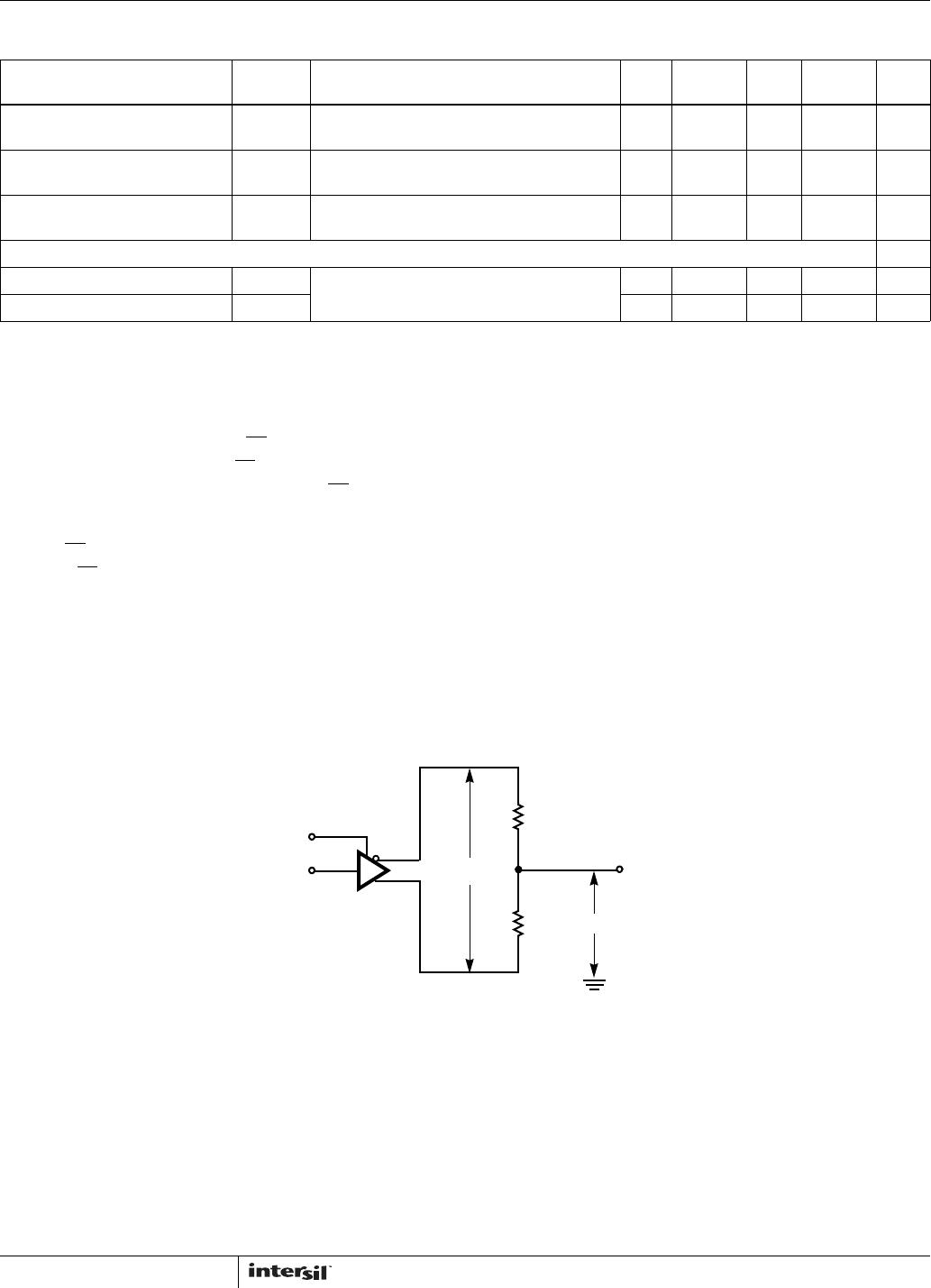
Driver Short-Circuit Current,
V
O
= High or Low
I
OSD1
DE = V
CC
, -7V V
Y
or V
Z
12V, (Note 4) Full 35 - 250 mA
Receiver Short-Circuit Current I
OSR
0V V
O
V
CC
Full 7 - 85 mA
SWITCHING CHARACTERISTICS (ISL8485E)
Driver Input to Output Delay t
PLH
, t
PHL
R
DIFF
= 54, C
L
= 100pF, (Figure 2) Full 18 30 50 ns
Driver Output Skew t
SKEW
R
DIFF
= 54, C
L
= 100pF, (Figure 2) Full - 2 10 ns
Driver Differential Rise or Fall Time t
R
, t
F
R
DIFF
= 54, C
L
= 100pF, (Figure 2) Full 3 11 25 ns
Driver Enable to Output High t
ZH
C
L
= 100pF, SW = GND, (Figure 3) Full - 17 70 ns
Driver Enable to Output Low t
ZL
C
L
= 100pF, SW = V
CC
, (Figure 3) Full - 14 70 ns
Driver Disable from Output High t
HZ
C
L
= 15pF, SW = GND, (Figure 3) Full - 19 70 ns
Driver Disable from Output Low t
LZ
C
L
= 15pF, SW = V
CC
, (Figure 3) Full - 13 70 ns
Receiver Input to Output Delay t
PLH
, t
PHL
(Figure 4) Full 30 40 150 ns
Receiver Skew | t
PLH
- t
PHL
| t
SKD
(Figure 4) 25 - 5 - ns
Receiver Enable to Output High t
ZH
C
L
= 15pF, SW = GND, (Figure 5) Full - 9 50 ns
Receiver Enable to Output Low t
ZL
C
L
= 15pF, SW = V
CC
, (Figure 5) Full - 9 50 ns
Receiver Disable from Output High t
HZ
C
L
= 15pF, SW = GND, (Figure 5) Full - 9 50 ns
Receiver Disable from Output Low t
LZ
C
L
= 15pF, SW = V
CC
, (Figure 5) Full - 9 50 ns
Maximum Data Rate f
MAX
(Note 11) Full 10 - - Mbps
SWITCHING CHARACTERISTICS (ISL8483E)
Driver Input to Output Delay t
PLH
, t
PHL
R
DIFF
= 54, C
L
= 100pF, (Figure 2) Full 250 800 2000 ns
Driver Output Skew t
SKEW
R
DIFF
= 54, C
L
= 100pF, (Figure 2) Full - 160 800 ns
Driver Differential Rise or Fall Time t
R
, t
F
R
DIFF
= 54, C
L
= 100pF, (Figure 2) Full 250 800 2000 ns
Driver Enable to Output High t
ZH
C
L
= 100pF, SW = GND, (Figure 3), (Note 5) Full 250 - 2000 ns
Driver Enable to Output Low t
ZL
C
L
= 100pF, SW = V
CC
, (Figure 3), (Note 5) Full 250 - 2000 ns
Driver Disable from Output High t
HZ
C
L
= 15pF, SW = GND, (Figure 3) Full 300 - 3000 ns
Driver Disable from Output Low t
LZ
C
L
= 15pF, SW = V
CC
, (Figure 3) Full 300 - 3000 ns
Receiver Input to Output Delay t
PLH
, t
PHL
(Figure 4) Full 250 350 2000 ns
Receiver Skew | t
PLH
- t
PHL
| t
SKD
(Figure 4) 25 - 25 - ns
Receiver Enable to Output High t
ZH
C
L
= 15pF, SW = GND, (Figure 5), (Note 6) Full - 10 50 ns
Receiver Enable to Output Low t
ZL
C
L
= 15pF, SW = V
CC
, (Figure 5), (Note 6) Full - 10 50 ns
Receiver Disable from Output High t
HZ
C
L
= 15pF, SW = GND, (Figure 5) Full - 10 50 ns
Receiver Disable from Output Low t
LZ
C
L
= 15pF, SW = V
CC
, (Figure 5) Full - 10 50 ns
Maximum Data Rate f
MAX
(Note 11) Full 250 - - kbps
Time to Shutdown t
SHDN
(Note 7) Full 50 200 600 ns
Driver Enable from Shutdown to
Output High
t
ZH(SHDN)
C
L
= 100pF, SW = GND, (Figure 3), (Notes 7, 8) Full - - 2000 ns
Electrical Specifications Test Conditions: V
CC
= 4.5V to 5.5V; Unless Otherwise Specified.
Typicals are at V
CC
= 5V, T
A
= +25°C, (Note 2) (Continued)
PARAMETER SYMBOL TEST CONDITIONS
TEMP
(°C)
MIN
(Note 12) TYP
MAX
(Note 12) UNITS
ISL8483E, ISL8485E
6
FN6048.10
September 3, 2015
Driver Enable from Shutdown to
Output Low
t
ZL(SHDN)
C
L
= 100pF, SW = V
CC
, (Figure 5), (Notes 7, 8) Full - - 2000 ns
Receiver Enable from Shutdown to
Output High
t
ZH(SHDN)
C
L
= 15pF, SW = GND, (Figure 5), (Notes 7, 9) Full - - 2500 ns
Receiver Enable from Shutdown to
Output Low
t
ZL(SHDN)
C
L
= 15pF, SW = V
CC
, (Figure 5), (Notes 7, 9) Full - - 2500 ns
ESD PERFORMANCE
RS-485 Pins (A/Y, B/Z) Human Body Model 25 - 15 - kV
All Other Pins 25 - >7- kV
NOTES:
2. All currents into device pins are positive; all currents out of device pins are negative. All voltages are referenced to device ground unless
otherwise specified.
3. Supply current specification is valid for loaded drivers when DE = 0V.
4. Applies to peak current. See “Typical Performance Curves” on page 10 for more information.
5. When testing the ISL8483E, keep RE
= 0 to prevent the device from entering SHDN.
6. When testing the ISL8483E, the RE
signal high time must be short enough (typically <200ns) to prevent the device from entering SHDN.
7. The ISL8483E is put into shutdown by bringing RE
high and DE low. If the inputs are in this state for less than 50ns, the parts are guaranteed
not to enter shutdown. If the inputs are in this state for at least 600ns, the parts are guaranteed to have entered shutdown. See “Low Power
Shutdown Mode (ISL8483E Only)” on page 9.
8. Keep RE
= V
CC
, and set the DE signal low time >600ns to ensure that the device enters SHDN.
9. Set the RE
signal high time >600ns to ensure that the device enters SHDN.
10. Devices meeting these limits are denoted as “single unit load (1 UL)” transceivers. The RS-485 standard allows up to 32 Unit Loads on the bus.
11. Limits established by characterization and are not production tested
.
12. Parameters with MIN and/or MAX limits are 100% tested at +25°C, unless otherwise specified. Temperature limits established by
characterization and are not production tested.
Test Circuits and Waveforms
FIGURE 1. DRIVER V
OD
AND V
OC
Electrical Specifications Test Conditions: V
CC
= 4.5V to 5.5V; Unless Otherwise Specified.
Typicals are at V
CC
= 5V, T
A
= +25°C, (Note 2) (Continued)
PARAMETER SYMBOL TEST CONDITIONS
TEMP
(°C)
MIN
(Note 12) TYP
MAX
(Note 12) UNITS
D
DE
DI
V
CC
V
OD
V
OC
R
R
Z
Y
ISL8483E, ISL8485E

ISL8485EIBZ

Mfr. #:
Manufacturer:
Renesas / Intersil
Description:
RS-422/RS-485 Interface IC 8LD -40+85 15KV HBM 5V RS-485 TRANS 1T
Lifecycle:
New from this manufacturer.
Delivery:
DHL FedEx Ups TNT EMS
Payment:
T/T Paypal Visa MoneyGram Western Union