16
Figure 23. 40 kBd propagation delay test circuit
Figure 26. Propagation delay test waveforms
Figure 25. Typical link propagation delay vs. optical powerFigure 24. Typical link pulse width distortion vs. optical power
5
3
4
2
1
-40 -28-34 -10
t – PULSE WIDTH DISTORTION – µs
D
6
0
-22 -16
P – INPUT OPTICAL POWER, dBm
R
5
3
4
2
1
-40 -28-34 -10
t – PROPAGATION DELAY – µs
P
6
0
-22 -16
P – INPUT OPTICAL POWER, dBm
R
7
8
t
PLH
t
PHL
17
Pin # Function
1 Anode
2 Cathode
3 Open
4 Open
5 Do not connect
8 Do not connect
Note: Pins 5 and 8 are for mounting and retaining purposes only. Do
not electrically connect these pins.
HFBR-15X3Z Transmitter
All HFBR-15XXZ LED transmitters are classied as IEC 825-1 Accessible Emission Limit (AEL) Class 1 based upon the current proposed
draft scheduled to go into eect on January 1, 1997. AEL Class 1 LED devices are considered eye safe. Contact your Avago sales
representative for more information.
Transmitter Electrical/Optical Characteristics 0°C to 70°C unless otherwise specied.
For forward voltage and output power vs. drive current graphs.
Parameter Symbol Min. Typ. Max. Units Conditions Ref.
Transmitter Output P
T
–11.2 –5.1 dBm I
Fdc
= 60 mA, 25°C Notes 3, 4
Optical Power –13.6 –4.5 I
Fdc
= 60 mA
–35.5 I
Fdc
= 2 mA, 0-70°C Fig. 9, 10
Output Optical Power ∆P
T
/∆T –0.85 %/°C
Temperature Coecient
Peak Emission λ
PK
660 nm
Wavelength
Forward Voltage V
F
1.45 1.67 2.02 V I
Fdc
= 60 mA
Forward Voltage ∆V
F
/∆T –1.37 mV/°C Fig. 18
Temperature Coecient
Eective Diameter D 1 mm
Numerical Aperture NA 0.5
Reverse Input Breakdown V
BR
5.0 11.0 V I
Fdc
= 10 µA,
Voltage T
A
= 25°C
Diode Capacitance C
O
86 pF V
F
= 0, f = 1 MHz
Rise Time t
r
80 ns 10% to 90%, Note 1
Fall Time t
f
40 I
F
= 60 mA
Note:
1. Rise and fall times are measured with a voltage pulse driving the transmitter and a series connected 50 Ω load. A wide bandwidth optical to
electrical waveform analyzer, terminated to a 50 Ω input of a wide bandwidth oscilloscope, is used for this response time measurement.
Absolute Maximum Ratings
Parameter Symbol Min. Max. Units Reference
Storage Temperature T
S
–40 +85 °C
Operating Temperature T
A
–40 +85 °C
Lead Soldering Cycle Temp. 260 °C Note 1, 4
Time 10 sec
Forward Input Current I
FPK
1000 mA Note 2, 3
I
Fdc
80
Reverse Input Voltage V
BR
5 V
Notes:
1. 1.6 mm below seating plane.
2. Recommended operating range between 10 and 750 mA.
3. 1 µs pulse, 20 µs period.
4. Moisture sensitivity level (MSL) is 3.
ANODE
1
CATHODE
2
N.C.
3
N.C.
4
8 DO NOT CONNECT
5 DO NOT CONNECT
For product information and a complete list of distributors, please go to our website: www.avagotech.com
Avago, Avago Technologies, and the A logo are trademarks of Avago Technologies in the United States and other countries.
Data subject to change. Copyright © 2005-2014 Avago Technologies. All rights reserved. Obsoletes 5989-4630EN
AV02-1501EN - September 19, 2014
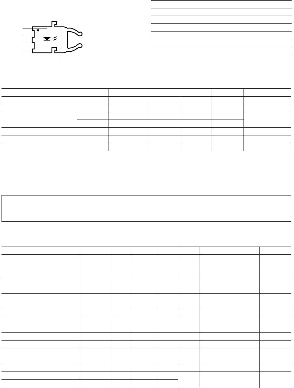
Pin # Function
1 V
O
2 Ground
3 Open
4 V
CC
5 Do not connect
8 Do not connect
Note: Pins 5 and 8 are for mounting and retaining purposes only.
Do not electrically connect these pins.
HFBR-25X3Z Receiver
Absolute Maximum Ratings
Parameter Symbol Min. Max. Units Reference
Storage Temperature T
S
–40 +85 °C
Operating Temperature T
A
–40 +85 °C
Lead Soldering Cycle Temp. 260 °C Note 1, 3
Time 10 sec
Supply Voltage V
CC
–0.5 7 V Note 2
Average Output Collector Current I
O
–1 5 mA
Output Collector Power Dissipation P
OD
25 mW
Output Voltage V
O
–0.5 7 V
Notes:
1. 1.6 mm below seating plane.
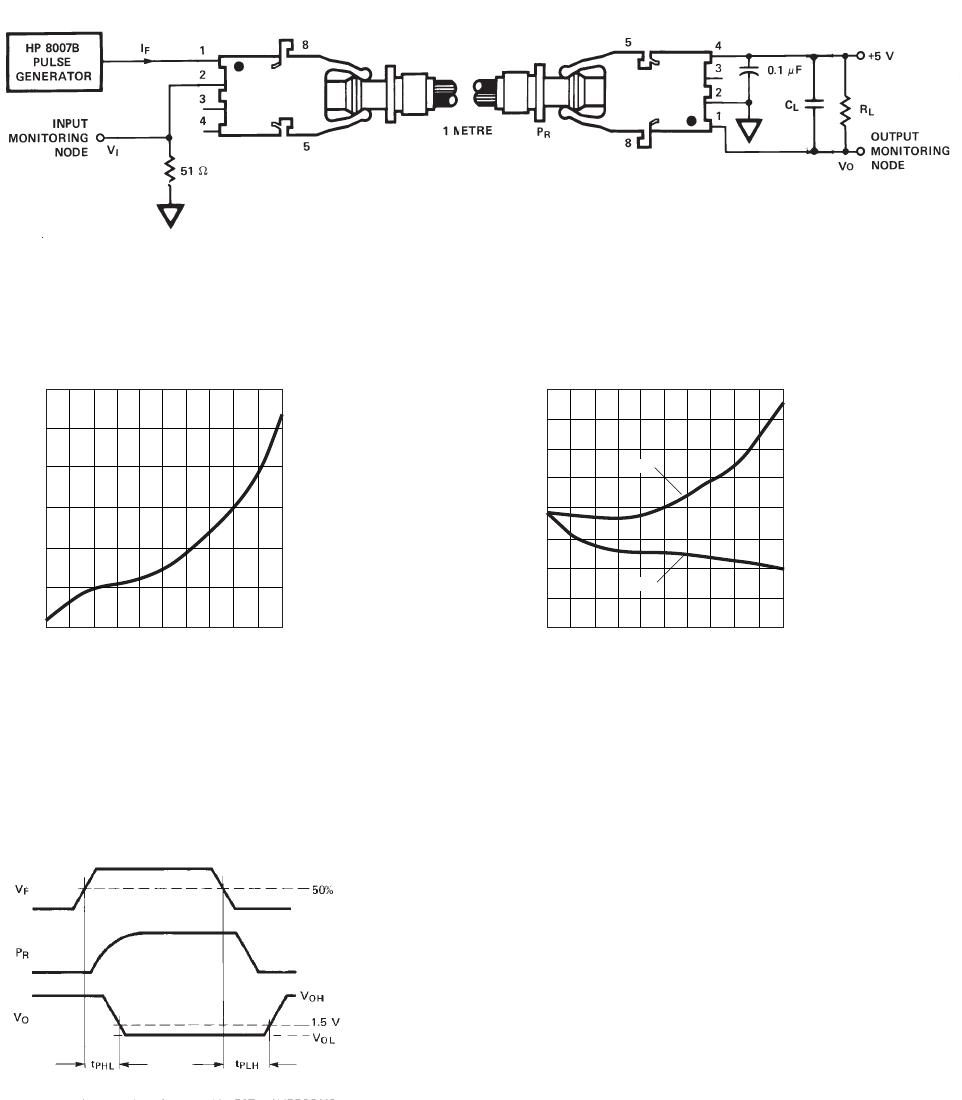
2. It is essential that a bypass capacitor 0.1 µF be connected from pin 2 to pin 4 of the receiver.
3. Moisture sensitivity level (MSL) is 3.
Receiver Electrical/Optical Characteristics 0°C to 70°C, 4.5 V ≤V
CC
≤5.5 V unless otherwise specied.
Parameter Symbol Min. Typ. Max. Units Conditions Ref.
Input Optical Power P
R(L)
–39 –13.7 dBm V
O
= V
OL
, I
OL
= 3.2 mA Notes 1,
Level Logic 0 –39 –13.3 V
O
= V
OL
, 2, 3
I
OH
= 8 mA, 25°C
Input Optical Power P
R(H)
–53 dBm V
OH
= 5.5 V Note 3
Level Logic 1 I
OH
= ≤40 µA
High Level Output Voltage V
OH
2.4 V I
O
= -40 µA, P
R
= 0 µW
Low Level Output Voltage V
OL
0.4 V I
OL
= 3.2 mA Note 4
P
R
= P
R(L)MIN
High Level Supply Current I
CCH
1.2 1.9 mA V
CC
= 5.5 V, P
R
= 0 µW
Low Level Supply Current I
CCL
2.9 3.7 mA V
CC
= 5.5 V, Note 4
P
R
= P
RL
(MIN)
Eective Diameter D 1 mm
Numerical Aperture NA 0.5
Notes:
1. Measured at the end of the ber optic cable with large area detector.
2. Optical ux, P (dBm) = 10 Log P(µW)/1000 µW.
3. Because of the very high sensitivity of the HFBR-25X3Z, the digital output may switch in response to ambient light levels when a cable is not
occupying the receiver optical port. The designer should take care to lter out signals from this source if they pose a hazard to the system.
4. Including current in 3.3 k pull-up resistor.
4
3
2
1
DO NOT CONNECT 5
DO NOT CONNECT 8
OPEN
V
CC
GROUND
V
O

HFBR-0503Z

Mfr. #:
Manufacturer:
Broadcom / Avago
Description:
Fiber Optic Development Tools DC-40KBd 650nm Evaluation Kit
Lifecycle:
New from this manufacturer.
Delivery:
DHL FedEx Ups TNT EMS
Payment:
T/T Paypal Visa MoneyGram Western Union