XRT8010
REV. 1.0.2
312MHZCLOCK&CRYSTALMULTIPLIERWITHLVDSOUTPUTS
6
1.0 CALIBRATION
The XRT8010 synthesizer jitter performance is optimized by calibration of its Voltage Controlled Oscillator
(VCO) upon initial power application. This power ON calibration procedure is automatic and completely trans-
parent to the user. It is initiated automatically upon first application of VDD. In order to bring the center fre-
quency of the VCO close to the desired output frequency, the VCO bias current is adjusted via a current DAC
at initial power application. The center frequency of VCO is checked against input reference frequency and cal-
ibrated internally to the desired output frequency value. These bias voltage trim bits are then held in latches for
as long as the VDD is held above 2.7V (minimum specified operational value of VDD). The user should note
the following important facts about this calibration procedure for proper operation of the XRT8010:
•
For proper operation of the chip and to achieve lowest jitter, the user should follow layout guidelines as
described in the User Guide.
•
An input crystal of appropriate frequency should be connected at XTAL1 and XTAL2 pins before power is
applied to the chip.
•
All VDD pins should be tied to 3.3V ±10% simultaneously.
•
The power supply should turn on without bouncing below 2.0V smoothly to its specified value in no more
than 50msec.
•
The calibration takes place during VDD ramp up between 2.6V to 3V values. Once the VDD reaches and
maintains 3.0V, the chip retains the calibrated VCO bias voltages in internal latches for proper operation.
•
To change a widely different value of crystal or input reference frequency, it is recommended to power
down the chip by bringing VDD to 0V and restarting after the change in frequency has occurred.
2.0 CRYSTAL SELECTION
It is recommended that a Fundamental Mode Crystal be used as the timing reference of the XRT8010. The fol-
lowing part has been qualified by EXAR:
CITIZEN Quartz Crystals
20 MHz : HCM49-20.000MABJT
40 MHz : HCM49-40.000MABJT
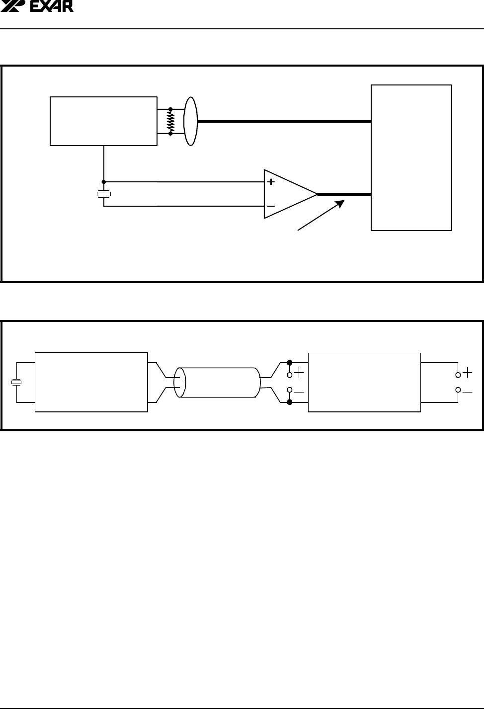
3.0 DATA AND PLOTS
All plots were recorded using the following parameters and test setup:
•
VDD = 3.3 V
• 2” 100Ω Differential Transmission Lines (from LVDS outputs to receiver inputs)
• Fundamental Mode Crystal of 20 MHz
• Vref = 1.5 V (PECL Receiver)
T
ABLE 3: POWER-DOWN AND OUTPUT TRI-STATE SELECTION TABLE
PD PIN 8OEPIN 7STATUS NOTES
1 X Outputs tri-stated and chip Powered-down “X” = don't care
0 1 Output tri-stated PD and OE have a 50KΩ pull-down resistor to ground
on chip