Data Sheet ADuM2200/ADuM2201
Rev. G | Page 5 of 17
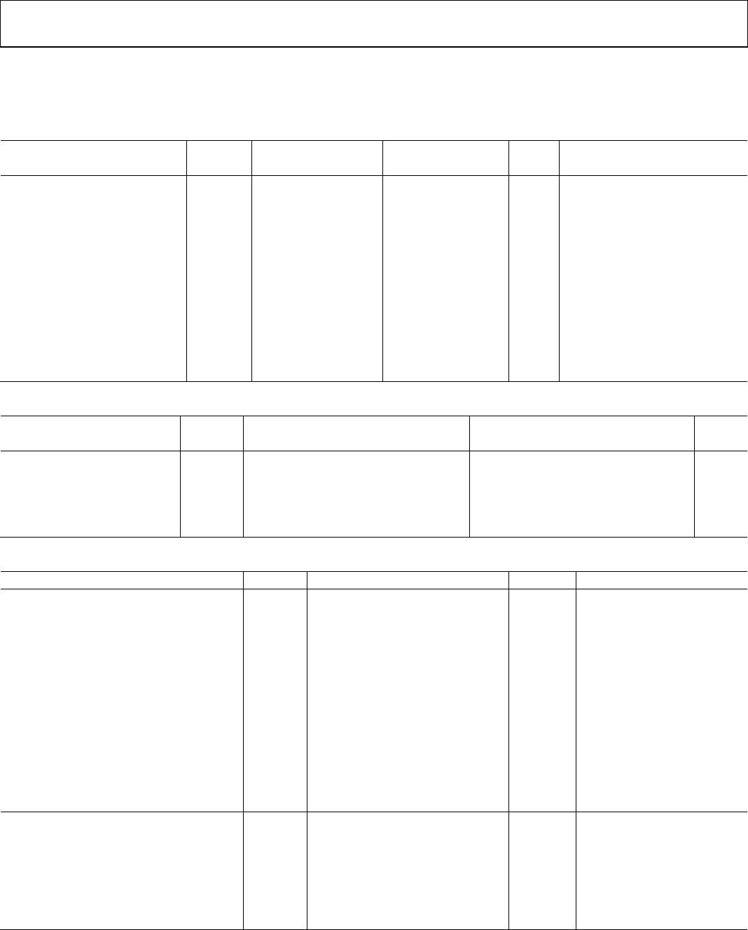
ELECTRICAL CHARACTERISTICS—MIXED 5 V/3.3 V OPERATION
All voltages are relative to their respective grounds. 4.5 V ≤ V
DD1
≤ 5.5 V, 3.0 V ≤ V
DD2
≤ 3.6 V. All minimum/maximum specifications apply
over the entire recommended operation range, unless otherwise noted. All typical specifications are at T
A
= 25°C, V
DD1
= 3.3 V, V
DD2
= 5.0 V.
Table 7.
A Grade B Grade Test Conditions/
Parameter Symbol Min Typ Max Min Typ Max Unit Comments
SWITCHING SPECIFICATIONS C
= 15 pF, CMOS levels
Pulse Width PW 1000 100 ns Within PWD limit
Propagation Delay t
, t
15 150 15 55 ns 50% input to 50% output
Pulse Width Distortion PWD |t
− t
|
A Grade and B Grade 40 3 ns
WA Grade and WB Grade 40 4 ns
Change vs. Temperature 5 ps/°C
Propagation Delay Skew t
50 22 ns Between any two units
Channel Matching
Codirectional t
50 3 ns
Opposing Directional t
50 22 ns
Table 8.
Parameter Symbol
1 Mbps—A Grade, B Grade 10 Mbps—B Grade
Unit Min Typ Max Min Typ Max
SUPPLY CURRENT (NO LOAD)
ADuM2200 I
1.3 1.8 3.5 4.6 mA
I
0.7 1.0 1.3 1.7 mA
ADuM2201 I
1.1 1.6 3.1 4.2 mA
I
0.8 1.6 1.9 2.5 mA
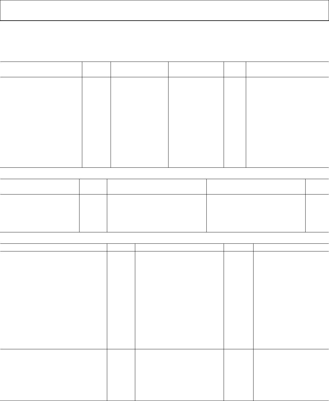
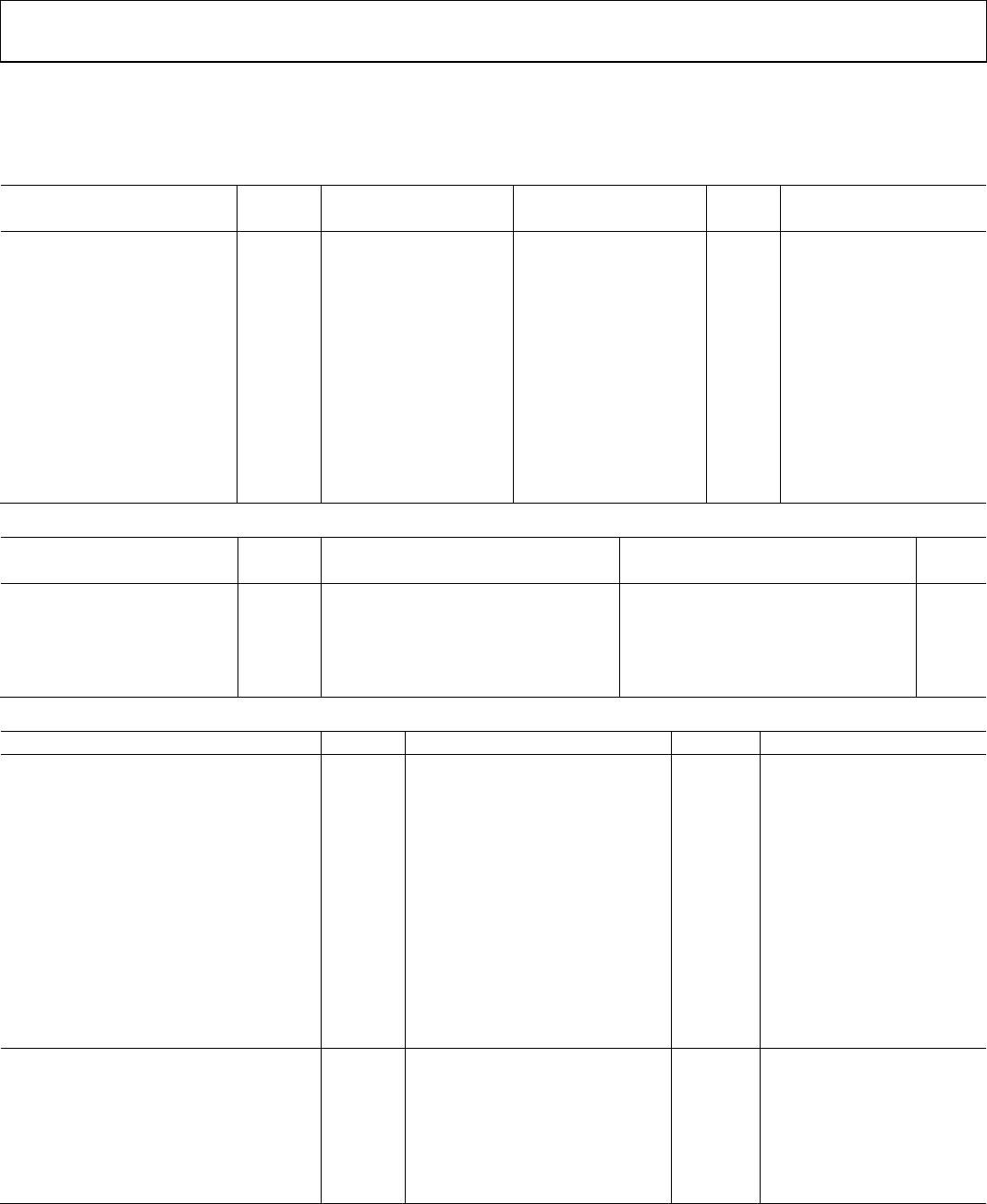
Table 9.
Parameter Symbol Min Typ Max Unit Test Conditions/Comments
1
DC SPECIFICATIONS
Logic High Input Threshold V
0.7 V
V
Logic Low Input Threshold V
0.3 V
V
Logic High Output Voltages V
V
− 0.1 V
V I
= −20 µA, V
= V
V
− 0.5 V
− 0.2 V I
= −3.2 mA, V
= V
Logic Low Output Voltages V
0.0 0.1 V I
= 20 µA, V
= V
0.2 0.4 V I
= 3.2 mA, V
= V
Input Current per Channel I
−10 +0.01 +10 µA 0 V ≤ V
≤ V
Supply Current per Channel
Quiescent Input Supply Current I
0.4 0.8 mA All inputs at logic low
Quiescent Output Supply Current I
0.3 0.5 mA All inputs at logic low
Dynamic Input Supply Current I
0.19 mA/Mbps
Dynamic Output Supply Current I
0.03 mA/Mbps
AC SPECIFICATIONS
Output Rise/Fall Time t
/t
10% to 90%
A Grade 10 ns
B Grade 3 ns
Common-Mode Transient Immunity
|CM| 25 35 kV/µs V
Ix
= V
DDx
, V
CM
= 1000 V,
transient magnitude = 800 V
Refresh Rate f
1.2 Mbps
1
I
Ox
is the Channel x output current, where x = A or B, V
IxH
is the input side logic high, and V
IxL
is the input side logic low.
2
|CM| is the maximum common-mode voltage slew rate that can be sustained while maintaining V
O
> 0.8 V
DD
. The common-mode voltage slew rates apply to both
rising and falling common-mode voltage edges.