2
Overview
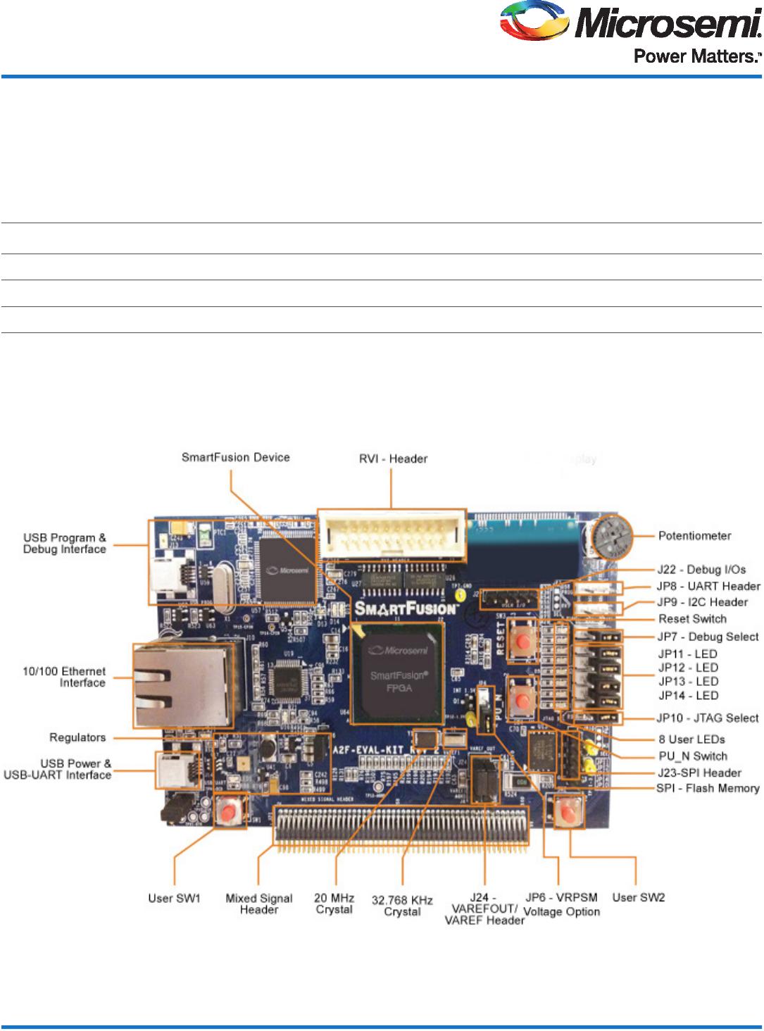
The Microsemi SmartFusion Evaluation Kit provides designers access to SmartFusion customizable SoC
FPGAs, the only devices that integrate an FPGA, an ARM
®
Cortex
®
-M3 processor, and programmable
analog, offering full customization, IP protection, and ease-of-use.
The device contains on-chip flash and on-chip SRAM memory, as well as additional SPI flash memory on
the board.
Pre-Programmed Demo Design
The SmartFusion Evaluation Kit comes with a preloaded Webserver demo design. If the board is
not preprogrammed, the programming file and the source files for the demo are provided on the
SmartFusion Evaluation Kit page. The source files are posted with the SmartFusion Webserver Demo
Using uIP and FreeRTOS document. See the Documentation Resources section for more information.
Running the Hardware Test Design
You can run the hardware test design to verify the device and board connections. The test design files
are available from the SmartFusion Evaluation Kit web page. Instructions on how to run the test are
available in the SmartFusion Evaluation Kit User’s Guide. See the Documentation Resource section for
more information.
Jumper Settings
Prior to powering up the SmartFusion Evaluation Kit for the first time, make sure the jumpers are in the
following positions.
Jumper Location Development Kit Function Setting
J6
2 pins next to Ethernet
jack
3.3 V Regulator 1–2
JP6 Next to PU_N switch VRPSM voltage option 2–3
JP7 Right side of board Input selecting option 1–2
JP10 Right side of board JTAG programming option 1–2
JP11 Right side of board Access to LED5 1–2
JP12 Right side of board Access to LED6 1–2
JP13 Right side of board Access to LED7 1–2
JP14 Right side of board Access to LED8 1–2
J24
Bottom right side of
board
VAREFOUT/ VAREF Header
1–2,
3–4
SmartFusion Evaluation Kit
Quickstart Card