IDT8N3SV75 Data Sheet LVPECL-FREQUENCY PROGRAMMABLE VCXO
IDT8N3SV75CCD
REVISION A NOVEMBER 19, 2013 12 ©2013 Integrated Device Technology, Inc.
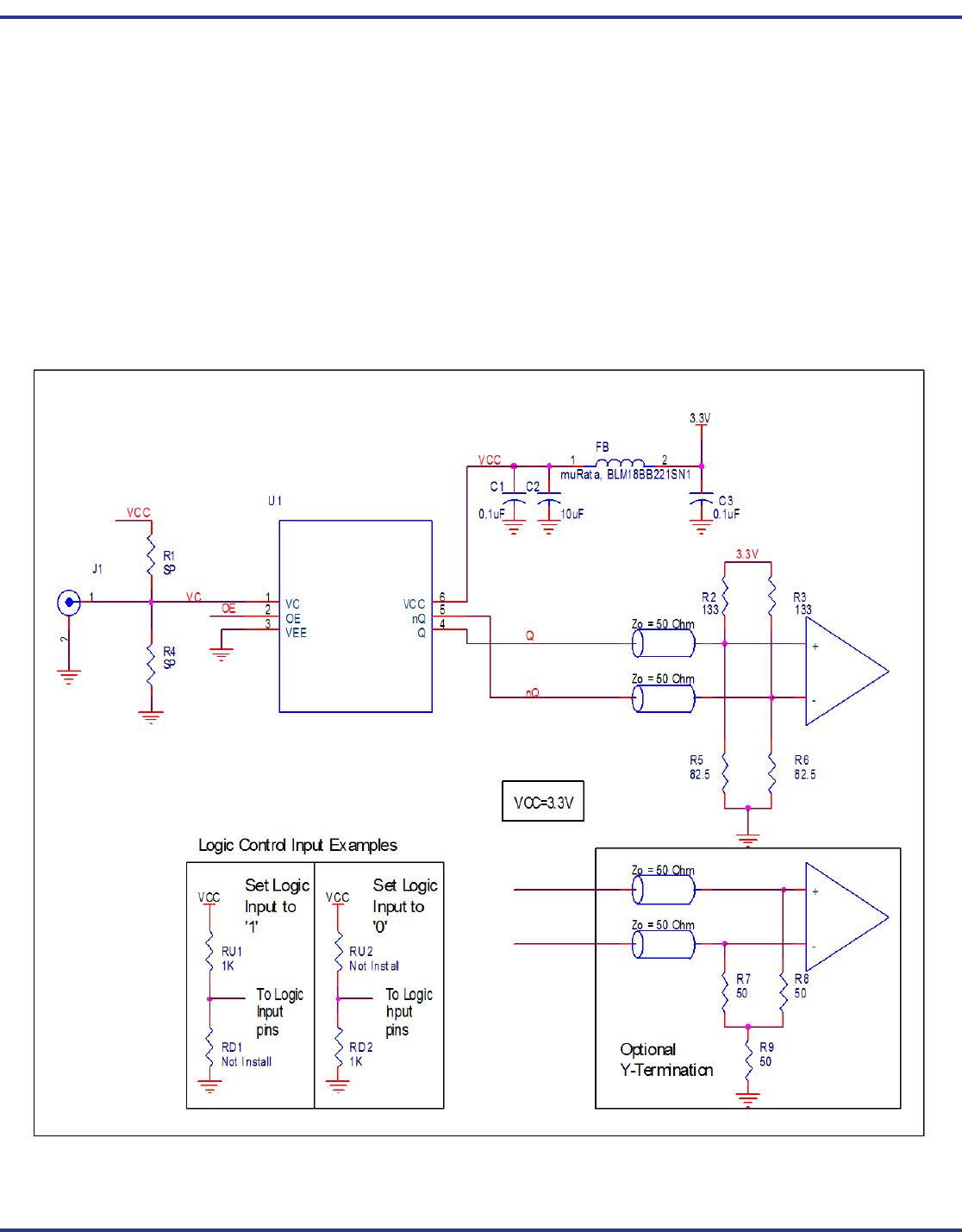
Schematic Layout
Figure 3 shows an example of IDT8N3SV75 application schematic.
In this example, the device is operated at V
CC
= 3.3V. As with any
high speed analog circuitry, the power supply pins are vulnerable to
random noise. To achieve optimum jitter performance, power supply
isolation is required.
In order to achieve the best possible filtering, it is recommended that
the
placement of the filter components be on the device side of the
PCB as close to the power pins as possible. If space is limited, the
0.1µF capacitor in each power pin filter should be placed on the
device side of the PCB and the other components can be placed on
the opposite side. Power supply filter recommendations are a general
guideline to be used for reducing external noise from coupling into
the devices. The filter performance is designed for a wide range of
noise frequencies. This low-pass filter starts to attenuate noise at
approximately 10 kHz. If a specific frequency noise component is
known, such as switching power supplies frequencies, it is
recommended that component values be adjusted and if required,
additional filtering be added. Additionally, good general design
practices for power plane voltage stability suggests adding bulk
capacitance in the local area of all devices.
The schematic example focuses on functional connections and is not
configur
ation specific. Refer to the pin description and functional
tables in the datasheet to ensure that the logic control inputs are
properly set.
Figure 3. IDT8N3SV75 Application Schematic