IDT8N3SV75 Data Sheet LVPECL-FREQUENCY PROGRAMMABLE VCXO
IDT8N3SV75CCD
REVISION A NOVEMBER 19, 2013 7 ©2013 Integrated Device Technology, Inc.
NOTE: Electrical parameters are guaranteed over the specified ambient operating temperature range, which is established when the device is
mounted in a test socket with maintained transverse airflow greater than 500 lfpm. The device will meet specifications after thermal equilibrium
has been reached under these conditions.
NOTE: XTAL parameters (initial accuracy, temperature stability, aging and total stability) are guaranteed by manufacturing.
NOTE: Characterized with V
C
=V
CC
/2.
NOTE 1: This parameter is defined in accordance with JEDEC standard 65.
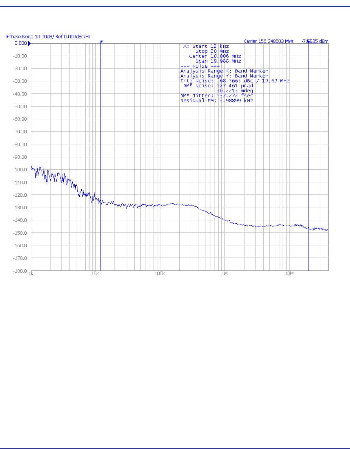
NOTE 2: Refer to the phase noise plot.
NOTE 3: Please see the FemtoClock NG Ceramic 5x7 Modules Programming guide for more information on PLL feedback modes and the
optimum configuration for phase noise.
NOTE: Electrical parameters are guaranteed over the specified ambient operating temperature range, which is established when the device is
mounted in a test socket with maintained transverse airflow greater than 500 lfpm. The device will meet specifications after thermal equilibrium
has been reached under these conditions.
NOTE 1: V
C
= 10% to 90% of V
CC
.
NOTE 2: Nominal oscillator gain: Pull range divided by the control voltage tuning range of 3.3V. E.g. for ADC_GAIN [6:0] = 000001 the pull
range is ± 12.5ppm, resulting in an oscillator gain of 25ppm ÷ 3.3V = 7.57ppm/V.
NOTE 3: For best phase noise performance, use the lowest K
V
that meets the requirements of the application.
NOTE 4: BSL = Best Straight Line Fit: Variation of the output frequency vs. control voltage V
C
, in percent. V
C
ranges from 10% to 90% V
CC
.
Table 5B. VCXO Control Voltage Input (V
C
) Characteristics, V
CC
= 3.3V ± 5% or 2.5V ± 5%, V
EE
=0V,T
A
= -40°C to 85°C
Symbol Parameter Test Conditions Minimum Typical Maximum Units
K
V
Oscillator Gain, NOTE 1, 2, 3 V
CC
= 3.3V 7.57 477.27 ppm/V
Oscillator Gain, NOTE 1, 2, 3 V
CC
= 2.5V 10 630 ppm/V
L
VC
Control Voltage Linearity; NOTE 4 BSL Variation -1 ±0.1 +1 %
BW Modulation Bandwidth 100 kHz
Z
VC
VC Input Impedance 500 k
VC
NOM
Nominal Control Voltage V
CC
/2 V
V
C
Control Voltage Tuning Range;
NOTE 4
0V
CC
V